【开源电机驱动】H 桥驱动-硬件篇
原文地址:http://www.modularcircuits.com/blog/articles/h-bridge-secrets/h-bridge_drivers/
本文翻译校正稿件,含有译者批注
H-Bridge Drivers
H 桥驱动-硬件篇
Introduction
引言
In the previous installment of the series we’ve gone through the high-level design decisions that you have to make when designing an H-Bridge, and we’ve discussed the considerations for selecting the MOSFETs and the catch diodes that will make up the bridge.
在本系列的前一部分中,我们已经讨论了在设计 h 桥时必须做出的高级设计决策,我们还讨论了选择 mosfet 和构成H桥的 c保护二极管的考虑因素。
In this article I will go through the available options for drive circuits. We will discuss the trade-offs between them and what influences the various parameters of the drive circuits.
在这篇文章中,我将展示可用的驱动电路选项。然后讨论它们之间的利弊以及不同参数对驱动电路的影响。
You will take the most out of this write-up if you are already fairly familiar with H-Bridge basics, so if you aren’t, I suggest you read the introductory piece of the series first. Understanding of the various drive-modes will also be useful, so reading the sign-magnitude drive, the lock anti-phase drive and the asynchronous sign-magnitude drive articles isn’t a waste of time either, though those pieces go into quite a bit of more detail than what is needed to follow this text.
如果您已经相当熟悉 H 桥的基础知识,那么您将从这篇文章中收益颇丰,因此如果您不熟悉 H 桥的基础知识,我建议您首先阅读该部分。它对理解各种驱动模式是有用的,因此阅读符号幅度驱动器、锁定反相位驱动器和异步符号幅度驱动器的文章也不是浪费时间,虽然这些文章有更多细节。
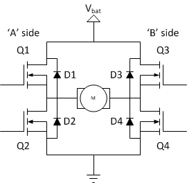
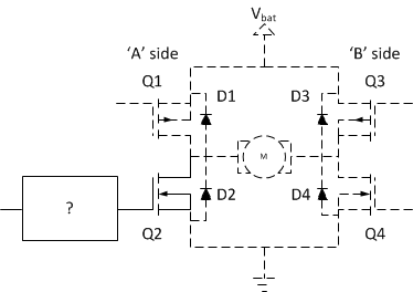
To make referencing easier, let’s review the H-Bridge circuit:
为了方便描述,让我们回顾一下H桥电路模型:
and our motor model:
还有我们的电机模型:

Drive circuitry
驱动电路
The drive circuitry for an H-Bridge is basically the electronics that sits between the PWM (and potentially other) digital control inputs and the MOSFET gates. It has two major purposes:
H 桥的驱动电路是指位于 PWM 以及其他数字控输出端和 MOSFET 栅极输入端之间的电子设备。它有两个作用:
- Translate the input voltages to suitable levels to drive the gates
- 将输入电平转换到合适的电压以驱动MOSFET的栅极
- Provide enough current to charge and discharge the gates fast enough
- 提供足够的电流,以更快的速度对栅极电容充放电(Ic = C*du/dt,t= C/Ic*U^2)
On top of that, many drive circuits include additional functionality:
除此之外,许多驱动电路还包括额外的功能:
- Translate the input command into gate-drive signals according to the drive mode
- 根据驱动模式将输入命令转换为栅极驱动信号
- Provide shoot-through protection
- 提供击穿保护
- Generate voltages for the high-side gate-drive circuitry (for N-channel drivers)
- 为高侧的栅极驱动电路(N沟道驱动器)产生驱动电压
- Provide additional safety functions, like over-current protection
- 提供额外的安全保护功能,如过流保护
- Control the turn-on and turn-off times of the FETs
- 控制 MOSFET 的开启和关闭时间
Drive circuits can come in many shape or form.
驱动电路可以有多种形式。
- There are low-side drivers, that are designed to drive Q2 or Q4 on our bridge.
- 低侧驱动器,用于驱动H桥的 Q2 或 Q4
- High-side drivers in turn are designed to drive Q1 or Q3.
- 高侧驱动器,用于驱动H桥的 Q1 或 Q3
- Half-bridge drivers combine one low- and one high-side driver, so they can drive Q1 and Q2 (or Q3 and Q4) together.
- 半桥式驱动器:结合了一个低侧和一个高侧驱动器,因此他们可以驱动 Q1和 Q2(或 Q3和 Q4)
- Full-bridge drivers obviously have two low-side and two high-side drivers so they can drive all four FETs.
- 全桥驱动器:显然有两个低侧和两个高侧驱动,所以他们可以驱动四个场效应管
As we’ve discussed in the previous article, low-side MOSFETs are always N-channel ones, while on the high-side we can you either P-channel or N-channel devices. This means that when we discuss high-side drivers (or half- and full-bridge drivers) we have to create two sub-categories, one for each channel-type.
正如我们在前一篇文章中所讨论的,低侧的 mosfet 总是 n 沟道的,而在高侧我们可以选择 p 沟道或 n 沟道。这意味着,当我们讨论高侧驱动程序(或半桥和全桥驱动程序)时,我们必须创建两个子类别,每种通道类型一个。
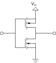
Before we dive into the details, let’s get familiar with the mother of all driver circuits, the complementer CMOS driver:
在我们深入讨论细节之前,让我们先熟悉一下所有驱动电路的原型,最完善的 CMOS 驱动:

In this circuit, a high-side PMOS and a low-side CMOS FET are combined to provide a clean digital logic output: if the input (the gates of the FETs) is grounded, the low-side FET is off, while the high-side is on. The output is connected to Vcc through the relatively low rrdson_high of the high-side element. When the input is connected to Vcc, the opposite happens, and the low-side FET starts conducting, while the high-side FET is off, so the output is connected to ground through a similarly low rdson_low. This topology is fairly common amongst not just bridge drivers, but logic gates and in general digital logic. We will use it as our starting example, and expand to more complicated circuits as we discuss the problems that come up.
该电路采用高端 PMOS 管和低端 CMOS 场效应管相结合的方式,提供了干净的数字逻辑输出: 如果输入端(FET 的栅极)接地,低端 FET 关闭,高端打开。输出通过高端元件的相对较低的rrdson_high连接到Vcc。当输入连接到Vcc时,情况恰好相反,并且低端FET开始导通,而高端FET关闭,因此输出通过类似的低rdson_low接地。 这种拓扑不仅在桥驱动器中而且在逻辑门和一般的数字逻辑中相当普遍。我们将使用它作为开始示例,并在讨论出现的问题时扩展到更复杂的电路。
In case you were wondering how is this driver stage different from one side of an H-bridge:
如果你想知道此驱动器与 H 桥的一侧有什么不同,下面就是答案:
- The FETs are much smaller, so their gate capacitance is really small. Even a relatively weak source can quickly charge and dis-charge them.
- 场效应晶体管要小得多,所以它们的栅极电容非常小。即使是相对较弱的电源也可以迅速充放电
- These smaller FETs also have a much higher rdson value (several ohms) so the dynamic shoot-through currents are low enough not be a headache.
- 这些小得多的FETs具有较高的rdson值(几欧姆) ,所以它的动态击穿电流很低,不是产生令人头疼的问题
This drive stage will be the building block for all of our low- and high-side drivers, but with some modifications on occasion. I’ll start with low-side drivers and discuss the problems you will face with them. Some of the discussion will be applicable (with slight changes) to high-side drivers. After those topics are cleared, we can continue on to high-side drivers.
该驱动器将成为我们所有低侧和高侧驱动器的基础,但会进行一些修改。 我将从低侧驱动程器开始,讨论将要面对的问题。 某些讨论将适用于高侧驱动器(稍有变化)。 缕清楚这些主题后,我们可以继续讨论高侧驱动器。
As I have said, this drive configuration is the same that is used in CMOS digital logic. (TTL and some other logic technologies are significantly different!) Because of this, as a concrete example, I’ll use the output stage of the AHC logic series to discuss the features and characteristics of this type of driver.
正如我已经说过的,此驱动器配置与CMOS数字逻辑中使用的驱动器配置相同。 (TTL和其他一些逻辑技术明显不同!)因此,作为一个具体示例,我将使用AHC逻辑系列的输出级来讨论此类驱动器的特性和特征。
Calculating turn-on and off times
计算开启和关闭时间
As we’ve discussed it in the previous part of the series, the gate capacitance of the MOSFETs together with the available drive current from the drive circuit will determine how fast the transistor can be turned on or off. Let’s investigate that topic a little more in detail!
正如我们在系列的前一部分所讨论的,mosfet 的栅极电容以及驱动电路中可用的驱动电流将决定晶体管的开关速度。让我们更详细地研究一下这个话题吧!
In the following I will only concentrate on a low-side, N-channel device and it’s driver. You can easily convert the results to a high-side drive situation for both the N- and P-channel cases.
下面我将集中讨论低侧,n 沟道元器件和它的驱动程序。您可以很容易地将结果转换到高侧的 n沟道 或者 p 沟道元器件。
FET datasheets specify the gate capacitance, sometime called the input capacitance. The capacitance varies a lot depending on the size of the device. For example, this relatively large MOSFET (the PHK31NQ03LT from NXP) has an almost 5nF gate capacitance. At the same time this transistor has a less than 5mΩ on-resistance. Another example would be IXTY 01N80. This 50mΩ on-resistance transistor only has a roughly 60pF gate capacitance.
FET 数据表指定了栅极电容,有时被称为输入电容。电容的大小取决于元器件的大小。例如,相对较大的 MOSFET (PHK31NQ03LT)具有接近5nF 的栅极电容。同时,这种晶体管的导通电阻小于5mΩ。另一个例子是 IXTY 01N80。这个50mΩ 导通电阻的晶体管只有大约60pF 的栅极电容。
To calculate the turn-on and off times we need to know a couple of things: how high the gate-voltage needs to be and how fast the drive circuitry can charge and discharge the gate-capacitance. Let’s address these questions in order: the minimum gate-voltage that is needed to turn the FET fully on is specified in the datasheet, but also depends on the drain current. It is usually specified in the form of a chart like this (this is from Wikipedia):
为了计算开通和关闭时间,我们需要知道两件事: 栅极电压需要多高,驱动电路栅极电容充放电的速度需要多快。让我们按顺序来解决这些问题: 数据表中规定了开启 FET 所需的最小栅极电压,但也取决于漏极电流。它通常是以这样的图表的形式指定的(来自维基百科) :
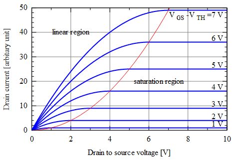
As you can see, for relatively low drain-currents (Y axis) the FET operates as a small resistance (the curve is linear and goes through the origin). For high currents however, the FET transitions into so-called saturation where the current is pretty much constant. For our application, we want to keep the FET in it’s linear (resistor-like) region. So, if you know the maximum current the FET (which is the current limit of the bridge), you can figure out the minimum gate-voltage that is needed to keep the FET linear. To take a practical example, let’s use the FDMS8880 FET and lets assume we want to build a bridge with a 20A current limit. The same diagram for this particular FET looks like this
正如你所看到的,对于相对较低的漏极电流(y 轴) ,FET 的工作特性相当于一个小电阻(曲线是线性的,通过原点)。然而,对于大电流而言,场效应晶体管过渡到所谓的饱和状态,通过的的电流几乎是恒定的。对于我们的应用,我们希望它保持在线性(电阻类)区。所以,如果你知道 FET 的最大电流(也就是电桥的极限电流) ,你就可以计算出保持 FET 线性所需的最小栅极电压。举一个实际的例子,假设我们使用 FDMS8880 FET,H桥的限制电流为20A 。这个特殊场效应管的相同图表如下所示:

You see that if the gate voltage (Vgs) is only three volts, the FET would not even be able to conduct 20A. It saturates at around 15A. With a gate voltage of 3.5V, you can get the device back into it’s linear region for 20A current, but it’s resistance is still a bit high. If you however increase the gate voltage to about 4.5V, you’ll see that the resistance at 20A does not depend on the gate voltage too much any more. So, for our case, we would need a gate voltage of at least 4.5V.
你可以看到,如果栅极电压(Vgs)只有3伏,FET 甚至不能传导20A。它在15A 左右达到饱和。当栅极电压为3.5 v 时,你可以让器件回到20A 电流的线性区域,但是它的电阻仍然有点高。如果你把栅极电压提高到4.5 v,你会发现20A 处的电阻不再太依赖于栅极电压。所以,对于我们的情况,我们需要至少4.5伏特的栅极电压。
让我们看一下我们使用的SED1007GG,它的栅极电压和能承载的电流关系如下图,假设我们的H桥需要承受10A的电流,那么我们需要至少6V的栅极电压,而在10A这个电流值,电阻都差不多,所以我们的栅极电压大于6V就可以了。取6.5V以上最佳。你也可以看到的是,当MOSFET上的电流超过40A时,MOSFET就在饱和区了,它是一条曲线。此外,从表中可以知道Vgs>10V,MOSFET就会完全开启,超过这个值太多的电压实际上没有必要了.

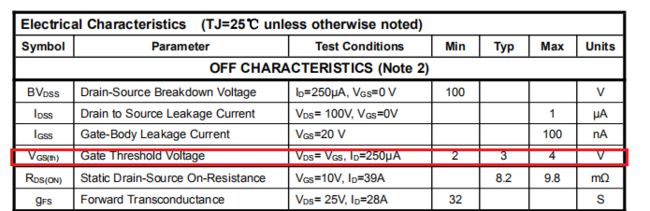
In order to turn the same FET off, we need to lower the gate voltage below the so-called threshold voltage(VGS(th)). This is again something that’s specified in the datasheet, for this particular device, it’s 1.2V (minimum).
为了关闭相同的场效应晶体管,我们需要降低所谓的阈值电压栅电压。这同样是在数据表中指定的VGS(th),对于这个特定的设备,它的最小值为1.2 v。而我们使用MOS,该值为3V。
Now, on to the second question: how fast can the driver charge or dis-charge the gate of the MOSFET. Driver characteristics are usually quite complex, and they are specified using charts, like this
现在,关于第二个问题: 驱动器能以多快的速度充电或放电的MOSFET的栅极。驱动特性通常是相当复杂的,它们是通过图表指定的,如下所示:
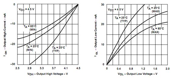
Here you see how the output current changes as the function of the output voltage, or the more useful way of looking at it: if you want to draw a certain amount of current out of the pin, how much the output voltage will deviate from its ideal value. This particular chart is from TI and specifies their AHC-series logic output characteristics (page 16). Notice how these charts are fairly similar to the charts above for MOSFET characteristics. This is not a coincidence, as the AHC series uses our complementer FET output drive circuit.
这里你可以看到输出电流是如何随着输出电压的变化而变化的,或者换一种说法: 如果你想从引脚中提取一定量的电流,输出电压会偏离它的理想值多少。这个特殊的图表来自 TI的 ahc 系列逻辑芯片(第16页)。注意,这些图表与上面的 MOSFET 特性图表非常相似。这不是一个巧合,因为 AHC 系列使用完整的 FET 输出驱动电路。
To approximate these curves, we can use a very simple model (again, using the MOSFET terminology): The output is in saturation mode for high currents – effectively acting as a current-source – and as the current decreases, it transitions into a linear region where it acts as a resistor. Graphically, we approximate the curve with two lines:

为了近似这些曲线,我们可以使用一个非常简单的模型(同样,使用 MOSFET 术语) : 输出是在饱和模式的大电流-有效地作为一个电流源-和当电流减少,它过渡到一个线性区域,它作为一个电阻器。在图形上,我们用两条线来近似曲线:
You can easily see that for the case of driving high voltages, the current source is at around 17mA, and the resistance is around 100Ω. When the output drives low, it can output 21mA and has roughly 70Ω resistance. (It is typical that an output stage has a somewhat weaker high-side driver, being a P-MOS device.)
您可以轻松地看到,对于驱动高侧,电流源输出约为17mA,等效电阻约为100Ω。 当输出驱动低侧时,它可以输出21mA电流并具有大约70Ω的等效电阻。 (通常,输出级的P-MOS器件的高端驱动器要弱一些。)
In many cases you can even further simplify the picture and assume either only the current-source or the linear region. We will go though all three approaches, using an example: as we’ve seen before, the FDMS8880 MOSFET can be turned on completely by a 4.5 or greater gate voltage. So, in theory it can be driven directly by a 5V digital pin. Let’s say we use the previously studied AHC-series to drive the gate of this transistor.
在许多情况下,您甚至可以进一步简化图片,并仅假设电流源或线性区域。 我们将以一个示例为例,介绍这三种方法:如前所述,可以通过4.5或更高的栅极电压完全打开FDMS8880 MOSFET。 因此,理论上它可以由5V数字引脚直接驱动。 假设我们使用先前研究的AHC系列来驱动该晶体管的栅极。
Constant current drivers
恒流驱动器
The constant current approach works the following way: we try to charge up a capacitor with a constant current source to (at least) a certain voltage. That will take some time:
恒流方法的工作原理如下: 我们尝试用恒流源给电容器充电至(至少)一定的电压。这需要一些时间:
Ton = Vgate * Cgate/Isource
其中 Vgate 是我们将 FET 完全打开需要的栅极电压,Cgate 是栅极电容,而 Isource 是驱动器可以提供的电流源。
由电容充电公式:t=Q/I=CU/I
The off-time could be calculated like this:
“关断时间”可以这样计算:
Toff = (Vgate-Vth) * Cgate/Isink
其中 Vth 是阈值电压。
Substituting the numbers for out example we get the following:
用这些数字代替我们的例子,我们得到如下结果:
Ton = 4.5 v * 1585pF/17mA = 419ns
Toff = (4.5V-1.2 v) * 1585pF/21mA = 249ns
Constant resistor drivers
固定电阻驱动器
The constant resistor approximation is more complex, because of the exponential response of the RC circuit. The turn-on time will be the following:
由于 RC 电路的指数响应特性,恒定电阻器的近似更为复杂。“导通”如下(这里把之前所说的栅极驱动等效电阻加上去了):
Ton =-Rsource * Cgate * ln (1-Vgate/Vsource)
其中 Rsource 为源电阻,Vsource 为驱动器的高级空载电压。
Similarly the off-time can be calculated as follows:
同样,“关断”时间的计算方法如下:
Toff =-Rsink * Cgate * ln (Vth/Vsource)
关于以上两个公式的推导过程:
我们使用以下模型,Vi为电压源,R与C串联。
充电过程:
由KVL:Vi = Ir*R + Vc = RC*dUc/dt + Uc,求解Uc = Ui*(1-e^(-1/RC)),于是t = -RC*ln(Ui - Uc)
详细过程:
①Vi = RC*dUc/dt 的通解为 A*e^(-t/RC)
②取t = 0,得一个特解为 Ui
③从而解为Uc = A*e^(-t/RC) + Us
④把Uc = A*e^(-t/RC) + Ui代入初始值t = 0,Uc = 0,可得0 = A + Ui,得 A = -Ui
⑤代入得Uc = -Ui*e ^(-t/RC) + Ui ,整理得Uc = Ui*(1-e^(-t/RC))
⑥于是t = -RC*ln(1-Uc/Ui)
其中τ = RC 被称为时间常数
放电过程:
放电过程等效于RC电路的零输入响应,假设电容已充满电,计算模型如下图所示:
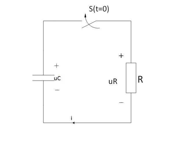
假设电容已经充满电,且Uc = U0
由KVL:Ur - Uc = 0,既 IcR - Uc = 0,代入Ic = -C*dUc/dt,我们得到RC*dUc/dt + Uc = 0
求解齐次微分方程,可得 Uc(t) = U0 * e^(-t/RC)
所以t = -RC*ln(Uc/Ui)
To be able to use this model for anything meaningful, we will have to assume that Vgate is lower than Vsource, in other words, the FET is fully on with a gate voltage that’s less the drivers no-load output voltage.
为了能够使用这个模型做任何有意义的事情,我们将不得不假设 Vgate 比 Vsource 低,换句话说,场效应晶体管完全处于开启状态,其栅极电压低于驱动器空载输出电压。
Doing the calculations for our example we get:
对我们的例子进行计算得到:
ton = –100Ω*1585pF * ln(1-4.5V/5V) = 364ns
toff = –70Ω*1585pF * ln(1.2V/5V) = 158ns
You can see that there’s quite a difference between the two estimations. Both are actually under-estimating the times: the constant current approach will assume more current than the driver can actually deliver at low output voltage drops, while the constant resistance approach (at least the way I did it here) over-estimates the current for the saturated region.
你可以看到这两种计算结果有很大的差异。这两种方法实际上计算的时间值都偏低: 恒定电流方法在低电压输出情况下栅极驱动器输出的电流大于栅极驱动器实际输出的电流,而恒定电阻方法(至少我在这里是这样做的)高估了饱和区域的电流。
Piece-wise linear model
分段线性模型
A more precise estimate can be made by combining the two methods, and assume constant current charge and discharge until the knee-point (2.9V and 1.4V respectively for our example) and assume constant resistance only for the remaining portion:
将两种方法结合起来可以得出更精确的估计,并假设恒流充电和放电直到膝点(我们的例子分别为2.9 v 和1.4 v) ,并假设恒电阻只适用于其余部分:
ton = Vknee_on*Cgate/Isource – Rsource*Cgate * ln(1-(Vgate-Vknee_on)/(Vsource-Vknee_on))
toff = (Vsource-Vknee_off)*Cgate/Isink – Rsink*Cgate * ln(Vth/Vknee)
With this approach, we get:
通过这种方法,我们可以得到:
ton = 497ns
toff = 286ns
These calculations can be done for P-channel MOSFETs and drivers as well, but of course you have to slightly change the equations to accommodate for the negative gate-source voltage of those devices.
这些计算也可以用于 p 沟道的 mosfet 和驱动器,当然你必须稍微改变一下方程,以适应这些器件的负的栅源电压。
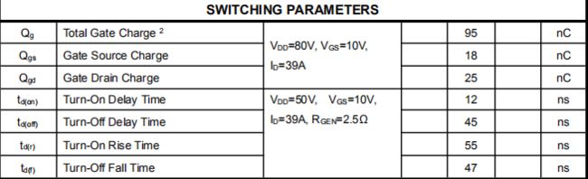
在目前的芯片数据手册中,厂家会给定MOS的开通关断时间以及栅极驱动器的通断时间,我们实际设计可以采用降额的方式来使用这些数据。MOS的数据表里显示,开通延时为12ns,开通上升时间为55ns,从而开通时间为12ns+55ns = 67ns,我们这里假设为高侧驱动,从数据表中可以知道栅极驱动器高端输出HO的Ton = 250ns,Tr = 120ns,从而栅极驱动器的开通时间为250ns + 120ns = 370ns,加上之前MOS的开通时间,整个高侧打开需要约67ns + 370ns = 437ns,可以看到与作者用数模型计算的结果类似。但是请读者注意,这是我们假设在栅极驱动器和mos的栅极之间没有串联额外电阻的情况。实际设计中我们需要这个电阻,下文会讨论这个问题。
 MOS的开通和关断时间
Controlling turn-on and off times
控制开启和关闭时间
So far so good, we have several ways now to calculate the transient times, with various accuracy. But what if you’re not satisfied with the results? What tools do you have to influence these numbers?
到目前为止结果还不错,我们现在有几种方法来计算瞬态时间,但他们具有不同的精度。但我们对这些结果并不满意?我们如何来要想这些数值呢?
If you want to make the time shorter, your pretty much have two choices: either change the FET to one with a lower gate capacitance or you change the driver to one that can provide more current.
如果你想缩短(开通或关断)时间,你有两个选择: 要么降低场效应管的栅极电容或者让驱动器可以提供更多的电流。
If you want to make the time longer, you have more options. One thing you can do is to add more capacitance to the gate by adding an extra capacitor towards ground for example.
如果你想增加(开通或者关断)时间,你有更多的选择。增加栅极电容或者在栅极和GND之间增加电容。
By far the most common way of controlling the trun-on and –off times is to add a series resistor to the driver outputs:
到目前为止,控制开启和关闭时间最常用的方法是在驱动器输出端串联电阻,如下图所示:
The series resistor method is ineffective if the driver is truly a current source, but that very rarely is the case. Normally, the effect is two-fold: one is that (by requiring more voltage for the same current) it gets the driver faster out of its current source region into it linear region. The second affect is that, once we’re in the linear region, the effective source resistance of the driver will be higher, so the time-constant of the charge-up or down of the capacitor will be larger.
如果驱动器是真正的电流源,串联电阻法是无效的。但是这样的情况很少。正常情况下,它们是相互影响的: 一是(相同电流情况下更高的电压)使驱动器可以更快地从电流源区进入线性区。第二个影响是,一旦我们进入线性区域,驱动器的有效源电阻就会增大,所以电容器充电上升或下降的时间常数就会增大。
Let’s see how to come up with the value of the resistor! If your model for the driver is a constant resistor one, the calculations are very simple: you simply express the required resistance from the on-time or off-time equations (here I’ll use the on-time one):
让我们来看看如何计算出电阻值!如果驱动程序的模型是一个常量电阻器,计算就非常简单: 你只需要从开机或关机时间方程表示所需的电阻(这里我将使用开机时间方程) :
ton = –(Rsource+Rg)*Cgate * ln(1-Vgate/Vsource)
so the needed series resistance is:
所以需要的电阻是:
Rg = -ton/(Cgate * ln(1-Vgate/Vsource))-Rsource
Note that if you do the same calculations for toff, you usually get a different Rg value. Since you need to select a single value, it means that you can’t independently control the on- and off-times.
注意,如果对 toff 进行相同的计算,通常会得到不同的 Rg 值。因为您需要选择一个值,这意味着您不能独立地控制开启和关闭时间。
If you used the combined current-source/linear model, you have a bit harder time, because first you have to figure out how long does the driver stay in current-source mode. The switch-over happens when the drive voltage is at it’s knee point – 1.4V or 2.9V in our case. However at that point the series resistor drop VRg = Rg*Isource voltage and only the rest is on the capacitor. So the time it takes to get out of the current-source region is this:
如果您使用的是组合的电流源/线性模型,那么您将会遇到一些困难,因为首先您必须计算出驱动程序在电流源模式下停留多长时间。在我们的例子中,当驱动电压在它的拐点:-1.4 v 或2.9 v 时,状态就会发生切换。然而,在这一点串联电阻下降 VRg = Rg * Isources,只有其余部分是在电容器上。因此,离开当前源区所需的时间如下:
ton_current_source = (Vknee_on – VRg)*Cgate/Isource
这里假设栅极驱动器是恒流源,因而栅极电阻将产生压降Vrg,而到达栅极电容两端的电压为Vknee_on - Vrg,再使用之前我们用于近似计算的公式
putting the above value in for VRg and doing some simplifications, we get:
将上面的值代入 VRg 并进行一些简化,我们得到:
ton_current_source = (Vknee_on/Isource – Rg)*Cgate
Similarly the time it takes to get out of the current-sink region for the turn-off time is:
类似地,在关闭时间离开当前汇聚区所需的时间是:
toff_current_sink = (Vsource/Isink-Vknee_off/Isink-Rg)*Cgate
After that time, the driver is in its linear (constant resistance) mode, so the previous equations can be used. The total turn-on and –off times for this approximation are the following:
在此之后,驱动器是在其线性(恒定电阻)模式,所以以前的方程可以使用。这个近似值的总开启和关闭时间如下:
ton = (Vknee_on/Isource – Rg)*Cgate – (Rsource + Rg)*Cgate * ln(1-(Vgate-Vknee_on)/(Vsource-Vknee_on))
toff = (Vsource/Isink-Vknee_off/Isink-Rg)*Cgate – (Rsink + Rg)*Cgate * ln(Vth/Vknee)
由经验值来看,Rg的值通常在0Ω-100Ω范围内,电阻越大,电桥打开所需要的时间就越长。让我们来做一个仿真,对比有Rj和无Rj,可以看到导通时间相差1us,也就是1000ns.
 Rj = 2K T= 10us
But what is the right turn-on or -off time after all?
但究竟什么是正确的开启或关闭时间呢?
After all this math you might ask this question. The problem is that there isn’t a clear-cut answer. The reasons you might want to lower the transients are the following:
经过这么多计算,你可能会问这个问题。然而没有一个明确的答案。你可能想要降低过渡期的原因如下:
- Reduced heat dissipation on the MOSFETs 减少 mosfet的热耗散
- More precise PWM control of the motor (the bridge spends less time in the not-so-well-defined transient states) 使用更精确的 PWM 控制电机(H桥在不确定过渡期的时间变短)
At the same time there are reasons to make the transients longer as well:
与此同时,也有理由使过渡期时间更长:
- The faster the transient is, the faster the catch diodes need to be 过渡时间越快,保护二极管的开关速度就越快
- Fast transients generate a lot of EMI noise 快速瞬变将产生大量的电磁干扰噪声
- Fast transients need high(er) current drivers 快速瞬变需要更大电流的驱动器
All in all, H-bridges are not the most demanding circuits as far as transient times are concerned: you’ve seen that a single AHC-series gate can pretty comfortably create sub-microsecond turn-on and –off times for a rather large FET. My guideline is that I try to keep the transient times to around 0.5-1% of the cycle time. This means that for a 20kHz bridge, I like to see 250-500ns transient times. This is a much more serious problem for higher switching frequencies that are normally found in high-power DC/DC converters, like PC motherboards.
总而言之,就瞬态时间而言,h 桥并不是要求最高的电路: 你已经看到,一个单一的 ahc 系列门可以非常轻松地为一个相当大的 FET 创造亚微秒的开关时间。我的经验是:尽量将过渡时间控制在周期时间的0.5-1% 左右。这意味着对于一个20kHz 的桥梁,我希望看到250-500ns 的过渡时间。对于更高的开关频率而言,这是一个更严重的问题,通常运用在在大功率 DC/DC 转换器中,如 PC 主板。
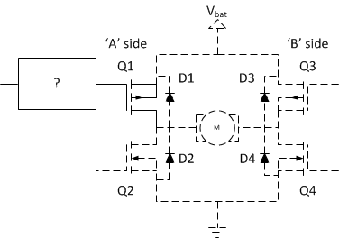
Low-side drivers
低端驱动
In the following I will only deal with one-half of the bridge. The second half needs identical treatment, so I’m going to ignore that for a while. On the low-side, we only have one type of device to deal with: N-channel FETs. These need a low voltage to turn them off, and a higher voltage (typically in the 5…15V range) to turn them fully on. The question is: what to put in the place of the mystery circuit:
在下面我将只处理桥的一半部分。后半部分与此相同,所以我暂时不会理会它。在H桥的低端,我们只有一种类型的器件来处理: n 沟道的场效应管。关闭它们需要一个低电压来,使他们完全打开需要较高的电压(通常在5-15V 范围内)。问题是: 在图中的问号上应该放置什么:
The simplest drive circuitry: none
最简单的驱动电路: 没有
For very simple, low-voltage designs, they might be completely missing, and the FETs are directly driven by logic level signals.
对于简单的低压设计,它们可以完全缺失,fet 直接由逻辑电平信号驱动。
This technique however only works under limited circumstances:
然而,这种方法只在有限的情况下才有效:
- You have to make sure that the output voltages of the digital logic are in fact capable of turning the FET fully on. This was true in out previous example, but if you’ve used lower-voltage logic (3.3V or even lower) or wanted to have higher currents through the bridge, it would not have been the case 你必须确保数字逻辑的输出电压是能够完全打开FET的 。在前面的例子中这是正确的,但是如果你使用了低电压逻辑(3.3 v 甚至更低)或者想要H桥能通过更高的电流,但是这不太现实。
- The logic output has enough current to generate the required turn-on and –off times. This is especially important for logic output with asymmetrical drive capabilities, like open-drain CMOS outputs or TTL chips. 逻辑输出具有足够的电流来产生所需的开启和关闭时间。这对于具有不对称驱动能力的逻辑输出特别重要,例如开漏 CMOS 输出或 TTL 芯片
Higher current drivers
更高的电流驱动器
If for the above reasons, you want to have a driver that can provide more current (but you’re still fine with the limited output voltage range), you can still use the complementer driver configuration, just use larger FETs, with lower rdson.
如果出于以上原因,你想要一个可以提供更多的电流(但你输出电压的范围仍然有限)的驱动,你可以使用完整的驱动器,只是使用尺寸较大的低 rdson的 fet,。
Alternatively, you can gang together several output buffers from standard CMOS devices to increase the drive capability that way, for example by connecting all six of the available inverters in an 74AHC04 together:
或者,你也可以将标准 CMOS 设备中的几个输出缓冲器组合在一起来提高驱动能力,例如将所有6个可用的逆变器连接到一个74AHC04上:

High-voltage complications
高压的复杂问题
So far we’ve only talked about low-side drivers where the voltage level of the gate-drive needed was within the range of standard digital logic. We’ve seen that – at least in that one example – a standard 5V digital logic gate works reasonably well for closing a relatively large MOSFET. As lower voltage (3.3V and below) digital standards gain popularity or if you try to increase the current capability of the bridge, you’ll find pretty quickly that direct logic level drive is inadequate.
到目前为止,我们只讨论了低端驱动器,其中所需的栅极驱动器的电压水平在标准数字逻辑的范围内。我们已经看到,至少在一个例子:一个标准的5V 数字逻辑门合理地工作,能够关闭一个相对较大的 MOSFET。随着低电压(3.3 v 及以下)数字标准的普及,或者如果你试图增加电桥的电流能力,你会很快发现直接逻辑电平驱动是不适当的。
When the gate-driver voltage of the FET is higher than your digital supply, at least a level-shifter will be needed in order to be able to drive the device. One of the simplest level shifters is this:
当 FET 的栅极驱动电压高于数字电源时,至少需要一个电平转换器来驱动器件。一个最简单的电压转换器是这样的:
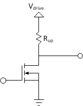
Here, the gate of the small-signal N-FET is driven by a suitable logic signal (and a logic level signal can easily turn this N-FET on) and the drain of it is pulled up to the gate-drive power supply, Vdrive. When the FET is off (the gate is driven to logic ‘0’), the output will be pulled to Vdrive by Rup. When the gate is driven to logic level ‘1’, the FET turns on, and pulls the output to 0V. So in fact, the output is the logical inverse of the input, but the voltage levels are changed to 0 and Vdrive.
在这里,小信号 N-FET 的栅极是由一个逻辑信号驱动的(逻辑电平信号可以很容易地打开这个 N-FET) ,它的漏极被拉到栅极驱动电源Vdrive上。当场效应管关闭(门驱动到逻辑‘0’) ,输出将由 Rup 拉到 Vdrive。当栅极驱动到逻辑电平“1”时,场效应晶体管打开,并将输出拉到0V。所以,事实上,输出是输入的逻辑逆,但电压水平被改变为0和 Vdrive。
The complication however is this: the drive strength (or current-delivery capability) of this level-shifter is significantly different in the ‘high’ and the ‘low’ case. When it drives low, its output resistance is pretty much rdson of the FET. When the output is high, it’s resistance is Rup. However Rup must be significantly higher than rdson otherwise the low-level output voltage would not be close to 0V. This in turn means that the turn-on time (which is determined by rdson for a P-FET) will be significantly – maybe even an order of magnitude – lower than the turn-off time, which is determined by Rup. This imbalance complicates shoot-through protection quite a bit and makes it very hard to turn the driven power FET off fast enough.
然而,复杂之处在于: 驱动强度(或电流驱动能力)的这个水平移动器是显着不同的“高”和“低”的情况。当它驱动器低,其输出电阻是相当大的栅场效应管。当输出是高的时候,它的阻力是 Rup。但是 Rup 必须明显高于 rdson,否则低电平输出电压将不会接近0V。这反过来意味着开启时间(这是由一个 P-FET 的开启时间决定的)将是显著的-甚至可能是一个数量级-低于关闭时间,这是由 Rup 决定的。这种不平衡复杂的射穿保护相当一点,并使它非常困难,以关闭驱动功率场效应晶体管足够快。
To overcome this problem, an complementer driver stage can be added between the level shifter and the power-FET:
为了解决这个问题,可以在电平转换器和功率场效应管之间增加一个完整的驱动:

This stage will make both the high- and low-level drive strength roughly equal, consequently making the turn-on and –off times much closer to one another.
这一阶段将使两个高和低水平的驱动强度大致相等,从而使开启和关闭时间更加接近彼此。
High-side P-MOS drivers
高端 P-MOS 驱动程序
So far we’ve only talked about driving N-MOS devices and driving them on the low-side. Let’s consider now the high-side drivers, first for P-MOS devices:
到目前为止,我们只讨论了驱动 N-MOS 器件和驱动他们的低侧驱动。让我们现在考虑高侧驱动,首先是 P-MOS 在高侧的情况:
This configuration present some complications: P-MOS transistors are open (non-conducting) when their gate is at close to the same potential as their source, and closed (conducting) when the gate is at a significantly lower potential, -5…-15V lower. This means that in order to completely turn off a high-side P-FET we’ll have to drive it’s gate as high as it’s source, which is connected to the power supply. To turn the FET on, we have to lower the gate voltage by 5…15V below Vbat.
这种结构带来了一些复杂性: 当 P-MOS 晶体管的栅极与源极电位接近时,P-MOS 晶体管处于开路(非导电)状态; 当栅极电位较低时,P-MOS 晶体管处于闭合(导电)状态,即Vgs = -5-15v。这意味着,为了完全关闭一个高侧的P-FET,我们将不得不使用与源极相同的高电压驱动它的栅极。为了打开 FET,我们必须将栅极电压降低5-15V,使它低于 Vbat。
All the drive circuits we’ve discussed before can be used for high-side P-FETs with the following change: you have to power the driver stage from the same voltage as the bridge is operating on, that is Vbat. That way, the high-level output voltage will be Vbat, which will turn the P-FET off properly, and the low-level output voltage will be 0, that is almost always enough to turn the FET on. (You might have problems with extremely low Vbat voltages, where you would have to drive the gate to a negative voltage to turn the FET on properly. This however is a rare enough case to ignore simply because high-current H-bridges usually operate at higher voltages and low-voltage H-bridges have low-enough currents that a small logic-level FET can be used in them that can be turned on by -Vbat.)
我们之前讨论过的所有驱动电路都可以用于驱动高侧 p 场效应管,但有些变化: 驱动的电源电压必须与电桥运行的电压相同,即 Vbat。这样,高电平输出电压必须是是 Vbat,才能使MOS管完全关闭,低电平输出电压必须是0,才能完全打开 FET。(如果你的 Vbat 电压特别低,你必须使驱动的电压为负电压才能正确地打开 FET。然而,这种情况几乎可以忽略忽略,因为大电流的 h 桥通常工作在较高的电压下,而低电压 h 桥的电流一般很低,在低压情况下,小型的场效应晶体管可以使用,它可以被 -Vbat 等级的电压打开。)
顺带一提,PMOS的栅极-源极电压必须为负值,MOS管才能被打开。假设我们使用3.3V的逻辑电平驱动MOS管,那么显然MOS的漏源极电压不能超过-Vgs + 3.3,如果Vbat >> 3.3V,那么无论栅极电压为高或者为低,都无法完全关闭PMOS,最多让他工作在线性区和非线性区。
Direct logic drive complications
直接逻辑驱动的复杂性
The additional limitation of the driver operating from Vbat has a significant consequence for direct logic-gate driven bridges: a simple AHC series gate, like the one we’ve used before will only be able to function in this role if the bridge power supply is lower than the maximum supply the gate itself can be operated from, that is, less than 5V. This is a very serious limitation as most bridges but the smallest ones operate from higher voltages to maximize power delivery without requiring enormous currents.
使用Vbat直接逻辑驱动H桥有一个严重后果:例如AHC系列逻辑门,就像我们以前使用的那样,只有当H桥的电源低于逻辑门本身可以操作的最大电压时,才能够起到这个作用,也就是说,5V的逻辑驱动能力小于5V。这是一个非常严重的限制,因为大多数电桥的工作电压很高,才能最大限度地而在不需要巨大的电流的情况下提供所需能量。(P =UI,同样功率,高电压意味着地底电流)
High-voltage drive complications
高电压驱动的附带问题
One of the major contributors to premature MOSFET deaths is gate-oxide break-down. The major cause of the breakdown is too high gate-source voltage on a MOSFET. The datasheets always specify this value, and for power MOSFETs at least the value is usually +/-20V. Getting out of this region will very quickly destroy the FET.
导致 MOSFET 过早失效的主要原因之一是栅极氧化层分解。这种失效方式称为“栅极电压失效”, MOSFET 的栅源极电压过高会发生这个问题。数据表会指定这个值,对于功率级别的 mosfet,这个值至少是 +/-20 v。超过这个范围将很快摧毁 FET。
This presents a problem for the high-side P-MOS drivers: if Vbat is higher than 20V, we can’t allow the gate drive to go down to 0V any more for low levels. It can go only as low as – say – Vbat-15V to allow for some safety margin as well. This is usually accomplished by adding a Zener diode to the drive circuit:
这对高端 P-MOS 驱动程序提出了一个问题: 如果 Vbat 大于20V,我们就不能允许门驱动程序在低电平下降到0V。它只能降到比如 Vbat-15V 这么低,以保证一定的安全裕度。通常通过在驱动电路中添加齐纳二极管来实现:
If you set the Zener voltage to about 15V, it will limit your voltage difference between the output and Vbat to be within the safe limits.
如果您使用的齐纳二极管的电压大约为15V,它将您的输出和 Vbat 之间的电压差限制在安全范围之内。
Similar limitations are needed on the low-side as well, if your driver works from Vbat and not from a separate power supply.
如果你的驱动也使用Vbat供电,而不是单独的电源,那么在低端也需要类似的限制。
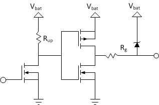
N-MOS high-side drive circuits
N-MOS 高侧驱动电路
So far we’ve only discussed driving P-MOS devices on the high-side. With all the complexities of level-shifting and voltage-limiting, P-MOS drivers are still simpler than drivers for an N-channel device.
到目前为止,我们只讨论了在高端驱动 P-MOS 器件。由于电平移位和电压限制的复杂性,P-MOS 驱动器仍然比 n 通道器件的驱动器简单。
The reason is the following: The source of an N-channel device on the high-side has to be connected to the motor terminal and its drain to the power supply, otherwise the body-diode would be forward-biased and would always conduct. To turn off an N-MOS device in that configuration, you can connect the gate to ground or to the source: gate-source voltage is going to be below or equal to 0. But where to connect the gate to turn on the device? The power supply is not enough, since, if the device is already conducting, it’s source and drain are roughly at the same potential. As the drain is connected to power, the source will be at that level as well, but than gate should be higher than that to keep the device on. We’ve seen that the gate should be at minimum 4.5V higher for our example above, and for some other devices maybe as much as 10-15V higher.
原因如下: 高端 n 通道器件的源极必须连接到电机端子,并将其漏极连接到电源上,否则体二极管就会正向偏置并导通。要关闭这种配置中的 N-MOS 器件,可以将栅极连接到地或源极: 栅极源极电压将低于或等于0。但是在哪里连接栅极来打开MOS呢?电源供应是不够的,因为,如果设备已经导通,它的源极和漏极大致在同一电位。由于漏极与电源相连,电源也将处于这一水平,但栅极应高于这一水平,以保持设备处于开启状态。我们已经看到,对于我们上面的例子来说,栅极应该至少超出4.5 v,而对于其他一些设备来说,可能超出10-15V。(高侧NMOS的源极连接的是电机一端,在工作时,漏极和源极电压是几乎相同的,而VGS需要大于4.5V,也就是以源极为参考,栅极电压需要高出4.5V,而对于地来讲,这个值是Vbat + 4.5V)
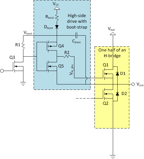
As Vbat is usually the highest voltage directly available in a system, this voltage needs to be generated. In most cases some kind of a charge-pump is used for that generation, mostly in a boot-strapped configuration:
由于 Vbat 通常是系统中直接可用的最高电压,因此需要产生这个栅极电压(Vbat + Vgs)。在大多数情况下,我们使用的是电荷泵,一般而言,电荷泵的启动配置如下:

While actual implementations could be quite a bit more complex, I will use this simplified variant to explain how things work. These circuits are usually operated form a voltage supply (Vcc) somewhere between 8 and 15V, for our discussion let’s say it’s working from 12V.
虽然实际的实现情况可能要复杂一些,但是我将使用这个简化的变体来解释它是如何工作的。这些电路的电压(Vcc通常为8到15V 之间),我们假设Vcc = 12V 。
This high-side driver shows strong similarities to the P-MOS high-side drivers we’ve discussed before, there are significant differences. While it also consists of a level-shifter (Q3, R1) followed by a C-MOS driver stage (Q4, Q5), this stage is neither grounded nor is connected to power. The lower leg of it is connected to the middle terminal of the bridge, or more importantly to the source of the power FET it drives, Q1. This means that the low-level output voltage of this stage (Vhi_drv) will be the same potential that the source of Q1 is, whatever that happens to be.
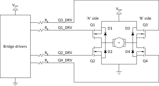
这种高侧驱动与我们之前讨论过得P-MOS 高侧驱动极其相似,但它也有一些明显的差异。虽然它也由一个电平转换器(Q3,R1)和一个C-MOS驱动器(Q4,Q5)组成,但它得输出级既不接地也不连接电源。而是连接到H桥的中间,更重要的是Vin_drv连接到它驱动的功率场效应晶体管Q1的栅极。这意味着它的低电平输出电压(Vhi_drv)将与Q1源极的电势相同,无论发生什么情况。(如下图所示,含有电荷泵的半桥驱动的连接示意,HO连接到MOS的栅极,VS连接到半桥的中间)
Let’s now see, what the voltage (Vboot) of the higher leg of the driver – that determines the high-level output voltage – is! To understand the operation of the circuit you’ll have to imagine that both the high- and the low-sides are driven by a PWM signal. We close Q2 for some portion of every cycle, and Q1 for the rest (not counting shoot-through protection for a minute).
现在让我们看看,驱动程序的较高端的电压(Vboot)是什么——它决定了高侧输出电压——是什么!为了理解电路的运作,你必须想象半桥的高端和低端都是由 PWM 信号驱动的。我们在每个周期的某些时刻导通Q2,在其余部分时刻导通 Q1(不包含击穿保护的时间)。
For the part of the cycle, when Q2 conducts, the output terminal voltage (Vout) is 0V, or very close to it. Since one side of Cbootis connected to this node, it is also grounded. Dboot, which is connected between Vcc and the other side of Cboot will make sure that Cboot is charged up to Vcc:
当 Q2导通时,输出端(Vout)与GND相连,电压接近0V。 Cboot 的右侧连接到Vout,所以它也接地。Vcc 通过防反二极管Dboot给 Cboot 充电,Cboot的电压上升到 Vcc(实际上是Vcc- Vf):
This of course also means that Vboot is equal to Vcc, 12V in our example. When it comes to turning Q2 off, Vout starts floating. Depending on what the motor, and the other side of the bridge does, either D1 or D2 will open and continue conducting the motor current.
所以,这也意味着 Vboot 等于Vcc也等于12V。当关闭 Q2时,Vout 开始浮空。桥的另一侧开始工作,D1或 D2将被打开继续传导电机电流。
If D2 openes, Vout would stay at 0V (actually it would go slightly negative for D2 to conduct, but let’s ignore that for now), so Cboot and Vboot stays as they were: charged up to Vcc, or 12V higher than Vout.
如果 D2开启,Vout 将保持在0V (实际上 D2的导通会略有压降,但我们暂时忽略这一点) ,所以 Cboot 和 Vboot 保持原样: 充电到 Vcc,或者比 Vout 高12V。
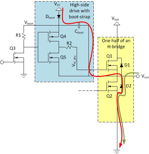
If we wanted to turn Q1 on at this point, Q4 can easily drive it’s gate 12V higher than it’s source terminal voltage (Vout), so we can clearly turn it on.
如果我们想在这一点上打开Q1,Q4可以很容易使Q1的栅极电压比它的源极电压(Vout)高出12伏,我们可以很容易的打开它。
If however D1 starts conducting after we turned Q2 on, Vout rises to Vbat (again, slightly higher, to forward-bias the diode, but I’ll ignore that here). When that happens – since the voltage across Cboot can’t change abruptly – Vboot has to rise and reach Vbat+Vcc. Normally, Cboot would discharge quickly towards Vcc, but in our case Dboot closes and lets Vboot rise as high as it wishes:
然而,如果 D1开始导电后,我们打开 Q2,Vout 电压将上升到 Vbat (再次上升,说是Vbat略微有点偏高,这里有二极管的正向偏置损失,但我会忽略这一点)。这种情况下——由于电容电压不能突然改变—— Vboot 会继续上升并到达 Vbat + Vcc。通常情况下,Cboot 会向 Vcc 快速放电,但是在我们的例子中,Dboot 会反向截止,让 Vboot 上升到它希望的电压水平:
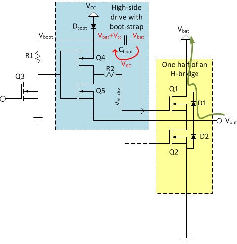
At that point Vout is at Vbat and Vboot is higher than that by Vcc (12V). If we wanted to turn Q1 on at this point, we can still do it: the high-level output voltage of the driver (Vboot) is 12V higher than the source voltage of Q1, as it is connected to Vout.
在这一点上,Vout 电压等于Vbat,而 Vboot 的电压比 Vcc高 (12V)。如果我们想在这一点上打开 Q1,我们仍然可以做到: 驱动(Vboot)的高电平输出电压比 Q1的源极电压高12V,因为它连接到 Vout。
All in all, Cboot and Dboot will make sure that Vboot is always at a higher voltage than Vout by Vcc. Or at least most of the time. The problem is that whenever Vboot is higher than Vcc, the only thing that keeps it at that level is the charge kept in Cboot. Any current that’s flowing out of that node will discharge the capacitor and eventually bring back Vboot to only Vcc. In our simple circuit, most of that current will flow through R1, but even if we solved that, other leakage currents through the various components will eventually do that. It takes a long time, probably seconds, but inevitably it will happen. What it means is that, while this circuit can certainly turn Q1 on, it can’t keep it turned on indefinitely.
总之,Cboot 和 Dboot 将确保 Vboot 始终比 Vcc 的 Vout 更高的电压。至少大多数时候是这样。问题在于,只要 Vboot 的电量高于 Vcc,唯一能使其保持在这个水平的就是 Cboot 的电量。任何电流流出该节点将放电的电容器,并最终带回 Vboot 只 Vcc。在我们简单的电路中,大部分的电流会流过 R1,但是即使我们解决了这个问题,其他通过各种元件的泄漏电流,最终也会这样做。这需要很长的时间,也许几秒钟,但是不可避免的会发生。这意味着,虽然这个电路肯定能够打开 Q1,但它不能无限期地保持打开状态。(Cboot称为自举电容,Dboot称为自举二极管)
The most important consequence is that bridges driven by this type of driver can’t operate at 100% duty-cycle: you’ll have to give some in every cycle for Cboot to re-charge.
最重要的是,这种类型的驱动器驱动的H桥不能以100% 的占空比运行: 因为你不得不在每个周期为Cboot重新充电。
As far as drive modes go, the circuit doesn’t put a significant limitation on the number of options available. For lock anti-phase drive, all four FETs are switching, so there is not problem at all, but for the two sign-magnitude drives, you’ll have to make sure that the FET that’s continuously on is on the low-side.
就驱动模式而言,这个电路并明显限制。对于锁定反相驱动器,所有四个场效应管都是需要切换的,所以没有问题,但对于两中符号幅值驱动方式,你必须确保低端的场效应管一直打开。
Another problem worth mentioning is this: when you try to turn Q1 on, that is you turn Q4 on, you basically connect Cboot and the gate-capacitance of Q1 in parallel. If Dboot is closed, so the only place to get charge to the gate is from Cboot, you are essentially just re-distributing the charge between the two capacitors. As that happens, the voltage on them will get lower, and the gate-voltage you can achieve depends on the ratio of the two capacitances:
另一个值得一提的问题是: 当你试图打开 Q1,也就是打开 Q4,你会串联 Cboot 和 Q1的栅极电容。如果 Dboot 是关闭的,那么栅极只有在 Cboot 上才能得到电荷,实际上你是在两个电容之间重新分配电荷。当这种情况发生时,它们(电容)上的电压会降低,而你能够达到的栅极电压取决于两种电容的比值:
Vgate = Vcc * Cboot / (Cboot + Cgate)
基本电路原理,电容串联,等流分压.
What this means is that if you want to make sure that Vgate is – let’s say – within 10% of Vcc, you have to make sure that Cboot is about an order of magnitude higher than the gate-capacitance of Q1. We’ve seen that the gate-capacitance of large FETs can be several nF, so Cboot should be in the 47-100nF range for those devices.
这意味着,如果你想确保 Vgate的电压在Vcc 的10% 范围以内波动,你就必须确保 Cboot 比 Q1的栅极电容高出大约1个数量级。我们已经看到,大型场效应晶体管的栅极电容可以达到几个 nF,因此对于这些设备来说,Cboot 应该在47-100nF 范围内。()
The last thing to talk about is that as the bridge is switching, Dboot keeps opening to top-up Cboot. But how much current will flow through it? As I’ve drawn the circuit above, the only thing limiting this current is the internal resistance of Dboot and the wires connecting them. All in all, there could be a significant current-spike on Vcc through Dboot due to the operation of the charge-pump. The power supply generating Vcc has a finite internal resistance, so this current-spike will translate into a periodic voltage drop on Vcc. To prevent that, usually a resistor is connected in series with Dboot to control the current flowing in the capacitor. It’s value is determined to make sure that you can completely re-charge Cboot even under worst-case duty-cycle conditions:
最后要讨论的是,随着H桥的不断切换,Dboot 会一直打开给Cboot充电。但是有多少电流会通过它呢?正如我在上面画的电路所示,唯一限制这个电流的是 Dboot 的内阻和连接它们的电线。总之,由于电荷泵的工作特性,Vcc 通过 Dboot 时可能会出现明显的电流尖峰。产生 Vcc 的电源具有有限的内阻,因此这个电流尖峰将转化为 Vcc 上的周期性电压降。为了防止这种情况,通常使用一个电阻器Rboot与 Dboot 串联,以约束在电容器中流动的电流。它的值必须确保在最糟糕的占空比条件下,也能重新给Cboot充完电:
Let’s say you allow for a maximum of 99% duty cycle, your gate capacitance is 5nF, Cboot is 100nF, Vcc is 12V and the operating frequency of the bridge is 20kHz. This means that you will charge the gate of Q1 up to 12V (disregarding now the voltage drop on Dboot and due to the charge-redistribution phenomena we’ve discussed above) 20000 times a second. Each time you charge the capacitor up, you need 5nF * 12V = 60nQ of charge. Since you do that 20000 times a second, the total charge transferred to the capacitor over a second is 1.2mQ, or in other words, your average gate-current is 1.2mA.
让我们假设你允许使用的最大占空比为99% ,栅极电容是5nF,Cboot 是100nF,Vcc 是12V,电桥的工作频率是20kHz。这意味着你将给 Q1的栅极充电到12V (不考虑 Dboot 上的电压降,也不考虑我们上面讨论过的电荷重新分配现象)每秒20,000次。每次你给电容器充电,你需要5nF * 12V = 60nQ 的电荷量。由于你每秒钟充电20000次,所以转移到电容器上的总电荷是1.2 mQ,换句话说,你的栅极的平均电流是 I = Q*t = 1.2mQ * 1s = 1.2 mA。
Let’s say (due to charge-redistribution and other leakage paths) under worst-case conditions Cboot looses 10% of its charge during the on-time. This results in a 1.2V drop on Vboot, that needs to be replenished during the off-time, which is (under worst-case conditions) 1% of the total cycle-time, or 500ns. To charge a capacitor of 100nF up by 1.2V in 500ns, you need 0.24A of (peak) charge current to do it.
让我们假设(由于电荷重新分配和其他泄漏路径)在最坏的情况下,Cboot在“导通”时间内失去10% 的电荷。这导致 Vboot 上的1.2 V 电压下降,需要在“关闭时间”内进行补充,这是(在最坏的情况下)总周期时间的1% ,或者说500ns。为了在500ns内给100nF 的电容器充电1.2 v,你需要0.24 a 的峰值充电电流。(T =-1/f = 1 / 20kHZ = 50us,50us * 1% =500ns,I = C*V/S = 100nF * 1.2/500ns = 0.24A)
From this quick calculation you see that the peak current (flowing through Rboot and Dboot) can be quite large compared to the modest average current flowing to the gate of Q1. This is important as this high current will stress your power delivery network, and can be a strong noise source for other parts of your design.
通过这个快速计算,你可以看到与流向Q1栅极的平均电流相比,峰值电流(流经 Rboot 和 Dboot)可以说是比较大的。这很重要,因为这个大电流会增加你的电力传输网络的负担,并且可能成为你设计的其他部分的一个强大的噪音来源。
Integrated drivers
综合型驱动器
We haven’t talked much about that so far, but the fact is that H-bridges and step-down DC/DC converters share a lot in common. So much so, that the driver circuits we’ve talked about here are the same that people use for high-current, synchronous DC/DC converters. Such converters are in use on PC motherboards these days, and that brought about an abundance of cheap and high-performance half-bridge drivers. These are almost exclusively of the boot-strap-based dual-N-channel MOSFET driver kind, but are equipped with additional goodies, like shoot-through protection, various input configurations, several voltage options, enable pins, built-in boost diode etc. They usually come in SO-8 packages, but of course other options are also available. You would need to use two of them to make a full bridge driver. Some examples include the L6743Q or L6387A from ST, the ADP3120A from OnSemi. You can also find full H-bridge drivers like the venerable – and expensive – HIP4081A from Intersil.
到目前为止,我们还没有对此进行过多的讨论,但事实上,h 桥和降压型 DC/DC 转换器有很多共同之处。我们在这里讨论的驱动电路,和用于大电流同步 DC/DC 转换器的驱动电路是一样的。这种转换器目前在主要用在PC 主板上,它带来了大量廉价和高性能的半桥驱动器。这些驱动器几乎是专用于驱动双 n 沟道 MOSFET ,但配备了额外的实用功能,如死区保护,各种输入配置,多种电压选项,使能引脚,内置自举升压二极管等。它们通常以 SO-8的封装形式出现,当然也有其他选择。你可以使用两个半桥驱动作为一个全桥驱动。比如 ST 的 L6743Q 或 L6387A,OnSemi 的 ADP3120A。您也可以找到全桥驱动,比如昂贵的Intersil的 HIP4081A 。
Conclusion
总结
This was a loooong article I have to admit, but hopefully it gives you some background into the design challenges of the drive circuitry of H-bridges. For all but the most simple applications, specialized drive circuitry is needed as while low-side drive is quite often possible from simple logic signals, high-side drive is usually more involved. Today, the availability of cheap, boot-strapped half-bridge driver ICs makes all N-channel bridges a very attractive design option.
我不得不承认,这是一篇很长的文章,但是我希望它能给你一些关于 h 桥驱动电路设计的背景知识。除了最简单的应用,使用专门的驱动电路是必要的,低侧驱动往往是可以使用简单的逻辑信号驱动的,而高侧驱动器通常很复杂。如今,廉价的,易用的半桥驱动芯片使所有 n 通道的H桥设计成为一个非常有吸引力的选择。
Now, that we’ve covered the basic construction of the bridges and their associated drive circuits, in the next installment of the series, we will look into the control of the bridge and some interesting variations on the previously established sign-magnitude and asynchronous sign-magnitude drive options.
现在,我们已经介绍了H桥的基本结构和相关的驱动电路,在本系列的下一部分中,我们将研究H桥的控制,以及之前讨论的符号幅值和异步符号幅值驱动方式的一些有趣的变化。