STM32存储左右互搏 SPI总线读写FLASH W25QXX
STM32存储左右互搏 SPI总线读写FLASH W25QXX
FLASH是常用的一种非易失存储单元,W25QXX系列Flash有不同容量的型号,如W25Q64的容量为64Mbit,也就是8MByte。这里介绍STM32CUBEIDE开发平台HAL库操作W25Q各型号FLASH的例程。
W25QXX介绍
W25QXX的SOIC封装如下所示,在采用SPI而不是QUAL SPI时,管脚定义为:
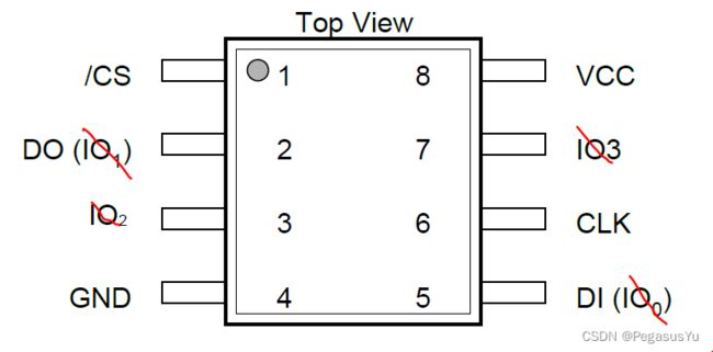
即由片选(/CS), 时钟(CLK), 数据输出(DO)和数据输入(DI)的组成4线SPI信号接口。VCC和GND提供电源和接地连接。
例程采用STM32H750VBT6芯片, FLASH可以选择为8/16/32/64/128/256/512/1024 Mbit的W25Q型号。
STM32工程配置
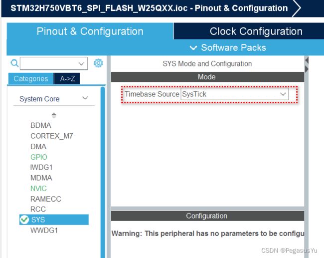
首先建立基本工程并设置时钟:

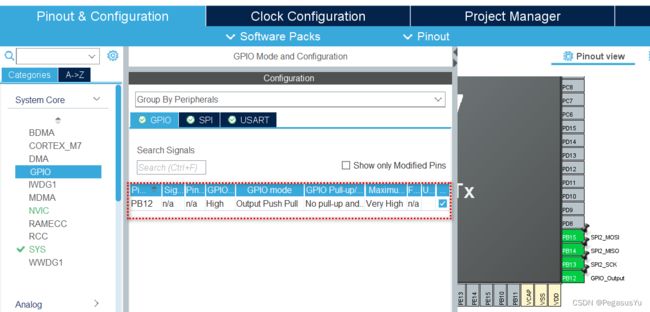
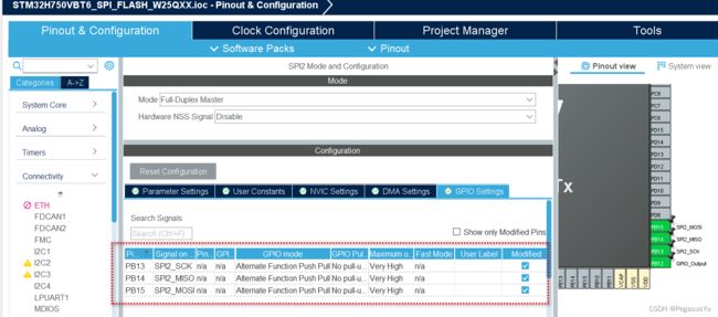
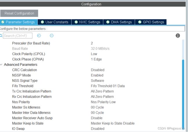
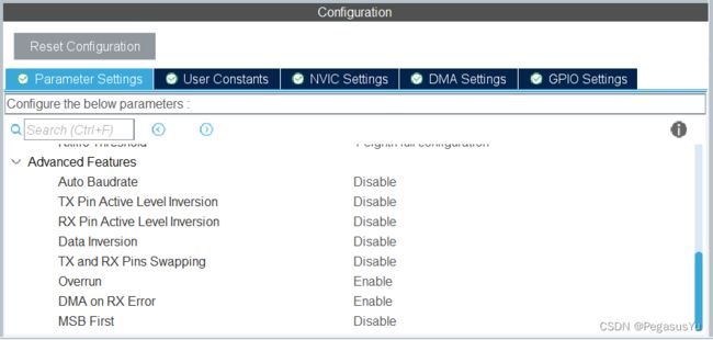
选择硬件接口SPI2为FLASH连接接口,片选采用软件代码控制方式,单独设置为输出GPIO:

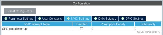
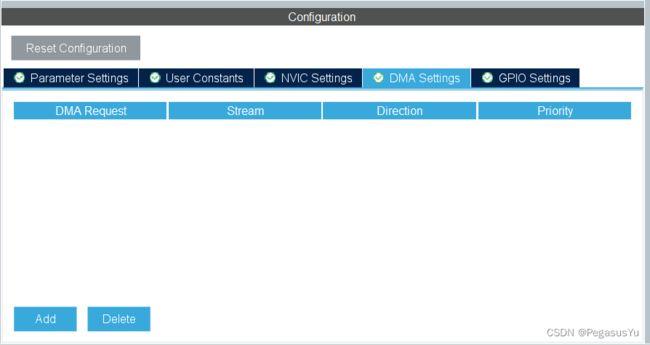
不采用中断和DMA方式,需要时可以再添加,调用相对应的操作库函数及补充中断处理函数即可。
配置UART1用于控制打印:


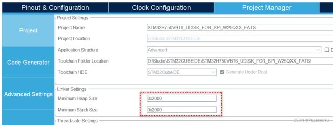
STM32H7资源较多,可以将堆栈开大:
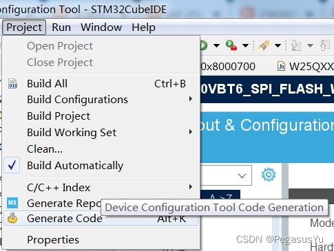
保存并生成初始工程代码:
STM32工程代码
UART串口printf打印输出实现参考:STM32 UART串口printf函数应用及浮点打印代码空间节省 (HAL)
建立W25Q访问的库头文件W25QXX.h:
#ifndef INC_W25QXX_H_
#define INC_W25QXX_H_

#include "main.h"

uint8_t SPI2_ReadWriteByte(uint8_t TxData);

//W25QXX serial chip list:
#define W25Q20_ID 	0XEF11
#define W25Q40_ID 	0XEF12
#define W25Q80_ID 	0XEF13
#define W25Q16_ID 	0XEF14
#define W25Q32_ID 	0XEF15
#define W25Q64_ID 	0XEF16
#define W25Q128_ID	0XEF17
#define W25Q256_ID	0XEF18
#define W25Q512_ID  0XEF19
#define W25Q1024_ID 0XEF20

extern uint16_t W25QXX_TYPE; //To indicate W25QXX type used in this procedure

//W25QXX chip select control function
#define W25QXX_CS(n)  ( n ? HAL_GPIO_WritePin(GPIOB, GPIO_PIN_12, GPIO_PIN_SET) : HAL_GPIO_WritePin(GPIOB, GPIO_PIN_12, GPIO_PIN_RESET) )

//command table for W25QXX access
#define W25X_WriteEnable		0x06
#define W25X_WriteDisable		0x04
#define W25X_ReadStatusReg1		0x05
#define W25X_ReadStatusReg2		0x35
#define W25X_ReadStatusReg3		0x15
#define W25X_WriteStatusReg1    0x01
#define W25X_WriteStatusReg2    0x31
#define W25X_WriteStatusReg3    0x11
#define W25X_ReadData			0x03
#define W25X_FastReadData		0x0B
#define W25X_FastReadDual		0x3B
#define W25X_PageProgram		0x02
#define W25X_BlockErase			0xD8
#define W25X_SectorErase		0x20
#define W25X_ChipErase			0xC7
#define W25X_PowerDown			0xB9
#define W25X_ReleasePowerDown	0xAB
#define W25X_DeviceID			0xAB
#define W25X_ManufactDeviceID	0x90
#define W25X_JedecDeviceID		0x9F
#define W25X_Enable4ByteAddr    0xB7
#define W25X_Exit4ByteAddr      0xE9

uint8_t W25QXX_Init(void);
uint16_t  W25QXX_ReadID(void);  	    		  //Read W25QXX ID
uint8_t W25QXX_ReadSR(uint8_t reg_num);           //Read from status register
void W25QXX_4ByteAddr_Enable(void);               //Enable 4-byte address mode
void W25QXX_Write_SR(uint8_t reg_num,uint8_t d);  //Write to status register
void W25QXX_Write_Enable(void);  		          //Write enable
void W25QXX_Write_Disable(void);		          //Write disable
void W25QXX_Write_NoCheck(uint8_t* pBuffer,uint32_t WriteAddr,uint16_t NumByteToWrite); //Write operation w/o check
void W25QXX_Read(uint8_t* pBuffer,uint32_t ReadAddr,uint16_t NumByteToRead);            //Read operation
void W25QXX_Write(uint8_t* pBuffer,uint32_t WriteAddr,uint16_t NumByteToWrite);         //Write operation
void W25QXX_Erase_Chip(void);    	  	                                                //Erase whole chip
void W25QXX_Erase_Sector(uint32_t Sector_Num);	                                        //Erase sector in specific sector number
void W25QXX_Wait_Busy(void);           	       //Wait idle status before next operation
void W25QXX_PowerDown(void);        	       //Enter power-down mode
void W25QXX_WAKEUP(void);				       //Wake-up


#endif /* INC_W25QXX_H_ */
建立W25Q访问的库源文件W25QXX.c:
#include "W25QXX.h"

extern SPI_HandleTypeDef hspi2;
extern void PY_Delay_us_t(uint32_t Delay);
//Write and read one byte in SPI2
uint8_t SPI2_ReadWriteByte(uint8_t TxData)
{
    uint8_t Rxdata;
    HAL_SPI_TransmitReceive(&hspi2,&TxData,&Rxdata,1, 1000);
 	return Rxdata;
}

uint16_t W25QXX_TYPE=W25Q64_ID;

//W25QXX initialization
uint8_t W25QXX_Init(void)
{
    uint8_t temp;

	W25QXX_CS(1);

	W25QXX_TYPE=W25QXX_ReadID();

    if((W25QXX_TYPE==W25Q256_ID)||(W25QXX_TYPE==W25Q512_ID)||(W25QXX_TYPE==W25Q1024_ID))
    {
        temp=W25QXX_ReadSR(3);              //read status register 3
        if((temp&0X01)==0)			        //judge address mode and configure to 4-byte address mode
		{
			W25QXX_CS(0);
			SPI2_ReadWriteByte(W25X_Enable4ByteAddr);
			W25QXX_CS(1);
		}
    }

    if((W25QXX_TYPE==0x0000)||(W25QXX_TYPE==0xFFFF)) return 0;
    else return 1;
}

//Read status registers of W25QXX
//reg_num: register number from 1 to 3
//return: value of selected register

//SR1 (default 0x00):
//BIT7  6   5   4   3   2   1   0
//SPR   RV  TB BP2 BP1 BP0 WEL BUSY
//SPR: default 0, status register protection bit used with WP
//TB,BP2,BP1,BP0: FLASH region write protection configuration
//WEL: write enable lock
//BUSY: busy flag (1: busy; 0: idle)

//SR2:
//BIT7  6   5   4   3   2   1   0
//SUS   CMP LB3 LB2 LB1 (R) QE  SRP1

//SR3:
//BIT7      6    5    4   3   2   1   0
//HOLD/RST  DRV1 DRV0 (R) (R) WPS ADP ADS
uint8_t W25QXX_ReadSR(uint8_t reg_num)
{
	uint8_t byte=0,command=0;
    switch(reg_num)
    {
        case 1:
            command=W25X_ReadStatusReg1;    //To read status register 1
            break;
        case 2:
            command=W25X_ReadStatusReg2;    //To read status register 2
            break;
        case 3:
            command=W25X_ReadStatusReg3;    //To read status register 3
            break;
        default:
            command=W25X_ReadStatusReg1;
            break;
    }
	W25QXX_CS(0);
	SPI2_ReadWriteByte(command);    //send command
	byte=SPI2_ReadWriteByte(0Xff);  //read data
	W25QXX_CS(1);
	return byte;
}

//Write status registers of W25QXX
//reg_num: register number from 1 to 3
//d: data for updating status register
void W25QXX_Write_SR(uint8_t reg_num,uint8_t d)
{
    uint8_t command=0;
    switch(reg_num)
    {
        case 1:
            command=W25X_WriteStatusReg1;    //To write status register 1
            break;
        case 2:
            command=W25X_WriteStatusReg2;    //To write status register 2
            break;
        case 3:
            command=W25X_WriteStatusReg3;    //To write status register 3
            break;
        default:
            command=W25X_WriteStatusReg1;
            break;
    }
	W25QXX_CS(0);
	SPI2_ReadWriteByte(command);            //send command
	SPI2_ReadWriteByte(d);                  //write data
	W25QXX_CS(1);
}
//W25QXX write enable
void W25QXX_Write_Enable(void)
{
	W25QXX_CS(0);
    SPI2_ReadWriteByte(W25X_WriteEnable);
	W25QXX_CS(1);
}
//W25QXX write disable
void W25QXX_Write_Disable(void)
{
	W25QXX_CS(0);
    SPI2_ReadWriteByte(W25X_WriteDisable);
	W25QXX_CS(1);
}

//Read chip ID
//return:
//0XEF11 for W25Q20
//0XEF12 for W25Q40
//0XEF13 for W25Q80
//0XEF14 for W25Q16
//0XEF15 for W25Q32
//0XEF16 for W25Q64
//0XEF17 for W25Q128
//0XEF18 for W25Q256
uint16_t W25QXX_ReadID(void)
{
	uint16_t Temp = 0;
	W25QXX_CS(0);
	SPI2_ReadWriteByte(0x90);          //send command
	SPI2_ReadWriteByte(0x00);
	SPI2_ReadWriteByte(0x00);
	SPI2_ReadWriteByte(0x00);
	Temp|=SPI2_ReadWriteByte(0xFF)<<8; //read high byte data
	Temp|=SPI2_ReadWriteByte(0xFF);    //read low byte data
	W25QXX_CS(1);
	return Temp;
}
//Read W25QXX from specific address for specific byte length
//pBuffer: data buffer
//ReadAddr: specific address
//NumByteToRead: specific byte length (max 65535)
void W25QXX_Read(uint8_t* pBuffer,uint32_t ReadAddr,uint16_t NumByteToRead)
{
 	uint16_t i;
	W25QXX_CS(0);
    SPI2_ReadWriteByte(W25X_ReadData);                   //send read command
    if((W25QXX_TYPE==W25Q256_ID)||(W25QXX_TYPE==W25Q512_ID)||(W25QXX_TYPE==W25Q1024_ID))   //send highest 8-bit address
    {
        SPI2_ReadWriteByte((uint8_t)((ReadAddr)>>24));
    }
    SPI2_ReadWriteByte((uint8_t)((ReadAddr)>>16));       //send 24-bit address
    SPI2_ReadWriteByte((uint8_t)((ReadAddr)>>8));
    SPI2_ReadWriteByte((uint8_t)ReadAddr);
    for(i=0;i<NumByteToRead;i++)
	{
        pBuffer[i]=SPI2_ReadWriteByte(0XFF);             //read data
    }
	W25QXX_CS(1);
}

//Write W25QXX not more than 1 page (256 bytes)
//pBuffer: data buffer
//WriteAddr: specific address
//NumByteToWrite: specific byte length (max 256)
void W25QXX_Write_Page(uint8_t* pBuffer,uint32_t WriteAddr,uint16_t NumByteToWrite)
{
 	uint16_t i;
    W25QXX_Write_Enable();                                       //write enable
	W25QXX_CS(0);
    SPI2_ReadWriteByte(W25X_PageProgram);                        //send write command
    if((W25QXX_TYPE==W25Q256_ID)||(W25QXX_TYPE==W25Q512_ID)||(W25QXX_TYPE==W25Q1024_ID))  //send highest 8-bit address
    {
        SPI2_ReadWriteByte((uint8_t)((WriteAddr)>>24));
    }
    SPI2_ReadWriteByte((uint8_t)((WriteAddr)>>16));               //send 24-bit address
    SPI2_ReadWriteByte((uint8_t)((WriteAddr)>>8));
    SPI2_ReadWriteByte((uint8_t)WriteAddr);
    for(i=0;i<NumByteToWrite;i++)SPI2_ReadWriteByte(pBuffer[i]);  //write data
	W25QXX_CS(1);
	W25QXX_Wait_Busy();
}

//Write W25QXX w/o erase check and w/o byte number restriction
//pBuffer: data buffer
//WriteAddr: specific address
//NumByteToWrite: specific byte length (max 65535)
void W25QXX_Write_NoCheck(uint8_t* pBuffer,uint32_t WriteAddr,uint16_t NumByteToWrite)
{
	uint16_t remained_byte_num_in_page;
	remained_byte_num_in_page=256-WriteAddr%256;                                                       //remained byte number in page
	if( NumByteToWrite <= remained_byte_num_in_page ) remained_byte_num_in_page = NumByteToWrite;      //data can be written in single page
	while(1)
	{
		W25QXX_Write_Page(pBuffer,WriteAddr,remained_byte_num_in_page);
		if(NumByteToWrite==remained_byte_num_in_page)break;                                            //end write operation
	 	else                                                                                           //NumByteToWrite>remained_byte_num_in_page
		{
			pBuffer+=remained_byte_num_in_page;
			WriteAddr+=remained_byte_num_in_page;

			NumByteToWrite-=remained_byte_num_in_page;
			if(NumByteToWrite>256)remained_byte_num_in_page=256;                                       //for whole page write
			else remained_byte_num_in_page=NumByteToWrite; 	                                           //for non-whole page write
		}
	};
}

//Write W25QXX w/ erase after check and w/o byte number restriction
//pBuffer: data buffer
//WriteAddr: specific address
//NumByteToWrite: specific byte length (max 65535)
uint8_t W25QXX_BUFFER[4096];
void W25QXX_Write(uint8_t* pBuffer,uint32_t WriteAddr,uint16_t NumByteToWrite)
{
	uint32_t secpos;
	uint16_t secoff;
	uint16_t secremain;
 	uint16_t i;
	uint8_t * W25QXX_BUF;
   	W25QXX_BUF=W25QXX_BUFFER;
 	secpos=WriteAddr/4096;                                        //sector number (16 pages for 1 sector) for destination address
	secoff=WriteAddr%4096;                                        //offset address in sector for destination address
	secremain=4096-secoff;                                        //remained space for sector
 	if(NumByteToWrite<=secremain)secremain=NumByteToWrite;        //data can be written in single sector
	while(1)
	{
		W25QXX_Read(W25QXX_BUF,secpos*4096,4096);                 //read sector data for ease necessity judgment
		for(i=0;i<secremain;i++)                                  //check sector data status
		{
			if(W25QXX_BUF[secoff+i]!=0XFF) break;                 //ease necessary
		}

		if(i<secremain)                                           //for ease
		{
			W25QXX_Erase_Sector(secpos);                          //ease sector
			for(i=0;i<secremain;i++)	                          //data copy
			{
				W25QXX_BUF[i+secoff]=pBuffer[i];
			}
			W25QXX_Write_NoCheck(W25QXX_BUF,secpos*4096,4096);     //write sector

		}
		else W25QXX_Write_NoCheck(pBuffer,WriteAddr,secremain);   //write data for sector unnecessary to erase

		if(NumByteToWrite==secremain)break;                        //for operation end
		else                                                       //for operation continuing
		{
			secpos++;                                              //sector number + 1
			secoff=0;                                              //offset address from 0

		   	pBuffer+=secremain;                                    //pointer adjustment
			WriteAddr+=secremain;                                  //write address adjustment
		   	NumByteToWrite-=secremain;				               //write number adjustment
			if(NumByteToWrite>4096) secremain=4096;	               //not last sector
			else secremain=NumByteToWrite;			               //last sector
		}
	};
}

//Erase whole chip, long waiting...
void W25QXX_Erase_Chip(void)
{
    W25QXX_Write_Enable();                  //write enable
    W25QXX_Wait_Busy();
  	W25QXX_CS(0);
    SPI2_ReadWriteByte(W25X_ChipErase);     //send erase command
	W25QXX_CS(1);
	W25QXX_Wait_Busy();   				    //wait for erase complete
}

//Erase one sector
//Sector_Num: sector number
void W25QXX_Erase_Sector(uint32_t Sector_Num)
{
 	Sector_Num*=4096;
    W25QXX_Write_Enable();                                     //write enable
    W25QXX_Wait_Busy();
  	W25QXX_CS(0);
    SPI2_ReadWriteByte(W25X_SectorErase);                      //send erase command
    if((W25QXX_TYPE==W25Q256_ID)||(W25QXX_TYPE==W25Q512_ID)||(W25QXX_TYPE==W25Q1024_ID))  //send highest 8-bit address
    {
        SPI2_ReadWriteByte((uint8_t)((Sector_Num)>>24));
    }
    SPI2_ReadWriteByte((uint8_t)((Sector_Num)>>16));           //send 24-bit address
    SPI2_ReadWriteByte((uint8_t)((Sector_Num)>>8));
    SPI2_ReadWriteByte((uint8_t)Sector_Num);
	W25QXX_CS(1);
    W25QXX_Wait_Busy();   				                       //wait for erase complete
}

//Wait idle status before next operation
void W25QXX_Wait_Busy(void)
{
	while((W25QXX_ReadSR(1)&0x01)==0x01);    //wait for busy flag cleared
}

//Enter power-down mode
#define tDP_us 3
void W25QXX_PowerDown(void)
{
  	W25QXX_CS(0);
    SPI2_ReadWriteByte(W25X_PowerDown);      //send power-down command
	W25QXX_CS(1);
	PY_Delay_us_t(tDP_us);                   //tDP
}
//Wake-up
#define tRES1_us 3
void W25QXX_WAKEUP(void)
{
  	W25QXX_CS(0);
    SPI2_ReadWriteByte(W25X_ReleasePowerDown);//send release power-down command
	W25QXX_CS(1);
	PY_Delay_us_t(tRES1_us);                  //tRES1
}
main.c文件操作代码里实现串口接收1个字节的指令,实现FLASH的ID读取,一页的写入,一页的读出三个功能。其它功能可以根据需要自行增加。
/* USER CODE BEGIN Header */
/**
******************************************************************************
* @file : main.c
* @brief : Main program body
******************************************************************************
* @attention
*
* Copyright (c) 2023 STMicroelectronics.
* All rights reserved.
*
* This software is licensed under terms that can be found in the LICENSE file
* in the root directory of this software component.
* If no LICENSE file comes with this software, it is provided AS-IS.
*
******************************************************************************
*/
//Written by Pegasus Yu in 2023
/* USER CODE END Header */
/* Includes ------------------------------------------------------------------*/
#include "main.h"
/* Private includes ----------------------------------------------------------*/
/* USER CODE BEGIN Includes */
#include "usart.h"
#include "W25QXX.h"
#include STM32例程测试
串口指令0x01测试效果如下:

串口指令0x02测试效果如下:

串口指令0x03测试效果如下:

STM32例程下载
STM32H750VBT6读写W25QXX例程下载
–End–