Zynq学习笔记:00 Vivado block diagram
系列视频:https://www.youtube.com/watch?v=UZ3FnZNlcWk
1. 新建工程,创建块设计并命名

Zynq SoC由PS(Processing System)和PL(Programmable Logic)组成,PL相当于FPGA,PS相当于CPU。
2. 创建PS部分:

(无需关注PS部分,在vivado中直接添加即可,我们关注的是关于PL部分的设计)
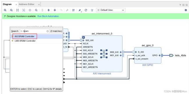
3. 添加IP:reset

slaves在左边,masters在右边:
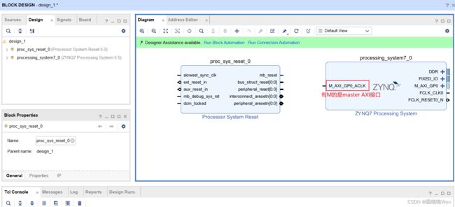
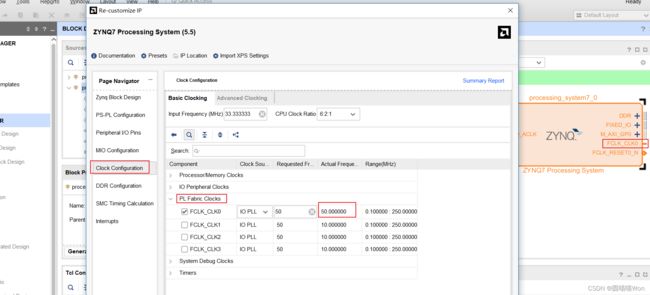
在processor中有一个时钟,processor给我们提供时钟:双击“Zynq Processing System”块,可以看到时钟配置:
可以看到处理器给PL fabric提供50MHz的时钟(从FCLK_CLK0引脚输出)
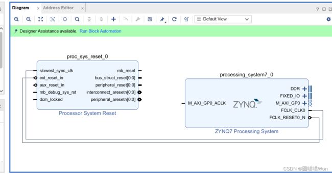
4. 时钟和时钟相连,处理器rst和外部rst相连(为PL fabric部分产生内部rst信号)
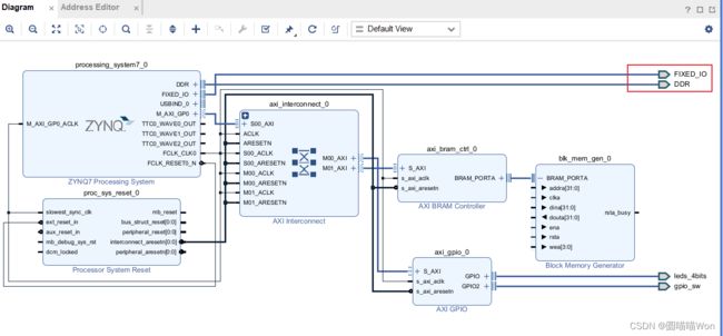
5. 添加AXI interconnect:
AXI interconnect是AXI memory mapped buses(AXI 内存映射总线)
every peripheral on the bus has an address (总线上的每个外设都有一个地址)
后面会在“地址编辑器”页面分配这些地址。可以通过扩展AXI总线去支持多master的设计。(因为可以有多个外设,可以在总线上放置多个外设,所以使用interconnect块去把单master变成2个AXI masters用来支持2个peripherals)

在interconnect块中有一个slave AXI,在processor块中有一个master AXI,将二者相连:

slave和master相连后,在总线(interconnect)上的每一个slave和master都有自己的时钟和reset信号。但是在这个例子里我们用统一的时钟和reset。

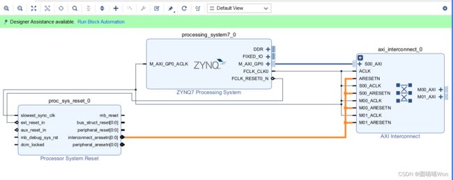
至此interconnect块已经连接完毕。
6.【vivado小tip】
如果已经在配置中选择了板子型号,不是选择device,是选择board,就会有board files,如下图所示:
双击LED,根据弹窗就可以知道什么IP核可以连接到这些LED上了。
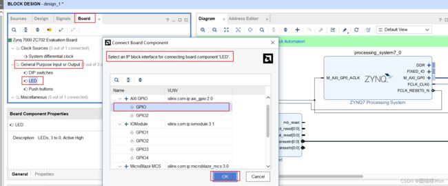
后面vivado会自动创建一个GPIO IP核并且和LED相连:
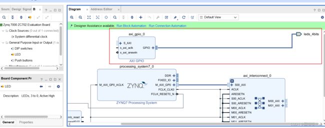
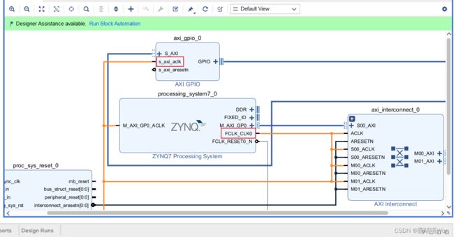
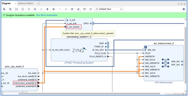
7. 将LED和AXI interconnect块相连,并连接时钟和reset信号:

右键重新排布:

8. 添加BRAM和block memory generator:

双击controller,配置如下:只有1个实例(instance),32比特宽:

之后连接好block RAM:


连接时钟和reset:

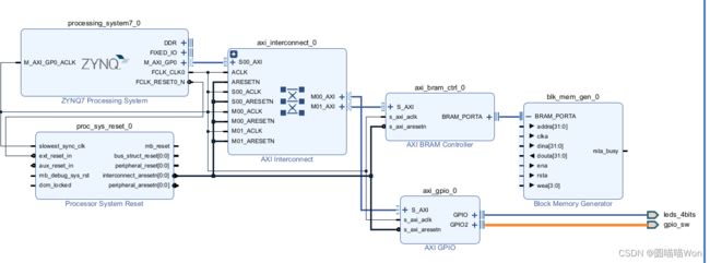
现在已经把2个peripherals(LED和BRAM)通过interconnect块和PS相连了。
processor可以使用AXI接口去控制LED和memory了。
GPIO:GPIO converts AXI register space into inputs and outputs. So in the output case, when we write from the processor into the AXI bus to this particular periphrals address that will turn that register write that value into signal outputs. In this way the processor can drive the LEDs.(GPIO:GPIO 将 AXI 寄存器空间转换为输入和输出。因此,在输出情况下,当我们从处理器写入 AXI 总线到这个特定的外设地址时,该寄存器将将该值写入信号输出。通过这种方式,处理器可以驱动 LED。)
添加一个switch:

现在,如果switch产生一个信号,这个信号会进入GPIO,GPIO会将信号通过AXI总线传输到processor。
block RAM controller给PL fabric添加block memory。在processor已经有memory的情况下,为什么还要在fabric添加memory呢?
Sometimes you want to have a register interface on your fabric, for example you have an algorithm or you have a module that needs to be configured, then having block memory in your fabric just makes it easier for your algorithm to access that memory, and that way you're saving up CPU memory for the CPU stuff. So I've added block memory which basically means the CPU can write to the memory at a specific address and then it wants to read from that memory you can do an AXI read and it'll get the data back. So it's like memory but it's on the fabric. (有时您希望在结构上有一个寄存器接口,例如您有一个算法或有一个需要配置的模块,那么在结构中拥有块内存只会使您的算法更容易访问该内存,并且这样你就可以为 CPU 的东西节省 CPU 内存。因此,我添加了块内存,这基本上意味着 CPU 可以写入特定地址的内存,然后它想要从该内存中读取数据,您可以执行 AXI 读取,然后它将取回数据。所以它就像记忆,但它在织物上。)
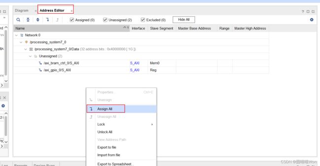
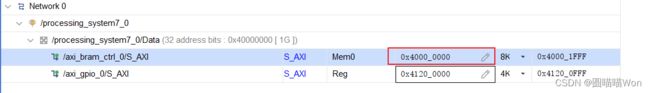
9. 为这些peripherals分配地址:
之前提到过,AXI是memory mapped protocol,这意味着每一个peripheral都需要一个地址。Address editor是我们在fabric中为peripherals分配地址的地方。
在address editor中右键,选择assign all:

可以看到地址范围:每个AXI peripheral都有一个base address,this is the address that's used by the CPU to access the periphral on the bus. In addition to the base address we also have a high address, and that's because periphrals don't just get one address they get a range of addresses. So these are the ranges of addresses that are assigned to these peripherals. (这是 CPU 用于访问总线上的外设的地址。除了基地址之外,我们还有一个高地址,这是因为外设不仅获得一个地址,而且还获得一系列地址。这些是分配给这些外设的地址范围。)
对于GPIO来说不需要那么多的内存,我们可以对其进行修改:
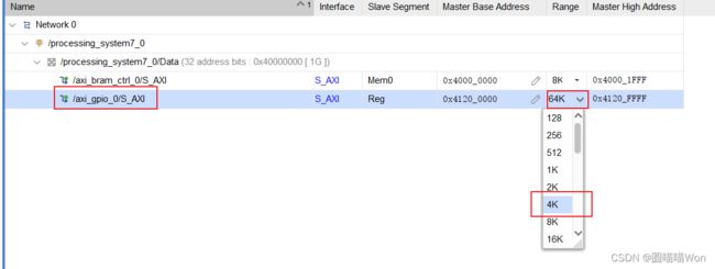
Fortunately for us these don't actually have any bearing on the actual memory usage, this is just how the bus is allocated. This isn't actually using up actual memory.(这些实际上对实际内存使用没有任何影响,这只是总线的分配方式。这实际上并没有耗尽实际内存。)
So when I write to this address, I'll be able to control the LEDs with the CPU. And when I write and read from this address, I'll be able to write values and read them back in the block RAM every byte has an address so if I have a 32-bit bus I have to increment by four to get the next 32-bit word. If we request an address that is a multiple of four that's called an align transfer if you request an address that's not a multiple of four it's called unaligned transfer. Generally we try to stick to align transfers. Some periphrals can't even handle unaligned transfers.(因此,当我写入该地址时,我将能够使用 CPU 控制 LED。当我从这个地址写入和读取时,我将能够写入值并将它们读回到块 RAM 中,每个字节都有一个地址,因此如果我有一个 32 位总线,我必须增加 4 才能得到下一个32 位字。如果我们请求的地址是四的倍数,则称为对齐传输;如果您请求的地址不是四的倍数,则称为未对齐传输。一般来说,我们会尝试坚持调整转移。有些外设甚至无法处理未对齐的传输)
10. run block automation(运行块自动化)
This is going to show us things that aren't connected yet and it's telling me that the IO and DDR on the PS need to be connected.(这将向我们展示尚未连接的东西,它告诉我 PS 上的 IO 和 DDR 需要连接。)

This is because there're some pins that need to be connected to the outside, the PS pins need to be connected to the outside so this is just rooting those PS pins straight to the outside.(这是因为有一些引脚需要连接到外部,PS 引脚需要连接到外部,所以这只是将这些 PS 引脚直接固定到外部。)
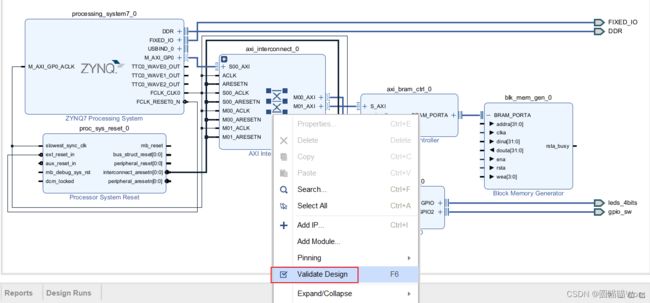
11. validate the design: check everything is OK.(验证设计:检查一切正常。)
12. generate bitstream:生成比特流文件
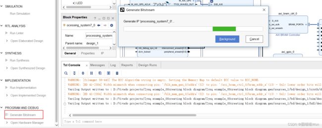
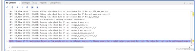
出现下列报错:
ERROR: [Common 17-70] Application Exception: Top module not set for fileset 'sources_1'. Please ensure that a valid value is provided for 'top'. The value for 'top' can be set/changed using the 'Top Module Name' field under 'Project Settings', or using the 'set_property top' Tcl command (e.g. set_property top
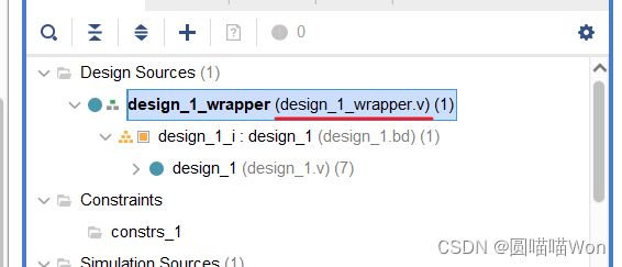
需要一个top level source:

如上图所示,the board file(*.bd) is the top level, but there is no board, so it's complaining. Vivado is saying: I want a top level file, that's not a block diagram. I want hardware description language in my top level please.(board design文件(*.bd)是顶层,但 Vivado 想要一个顶级文件,而不是框图。Vivado需要顶级硬件描述语言。)
解决办法:
右键,点击 create HDL wrapper。What this is going to do is we're going to take my block diagram and going to wrap it up into hardware description for me. (这样做的目的是,我们将获取框图并将其包装成硬件描述。)

现在top level file是HDL文件了。
This is also really helpful if you have other hardware description code, typical system verilog or VHDL code that you want to include in this project alongside a block diagram.(如果想要将其他硬件描述代码、典型系统 verilog 或 VHDL 代码与框图一起包含在该项目中,这种方法也非常有帮助。)
This *_wrapper.v file is like a literal verilog file you can put in your own modules here that can talk to the block diagram interface with each other and include that code in your project. So this is really nice if you want to use the block diagram but you also have your own code that you've written and that you want to use alongside it.(这个 *_wrapper.v 文件就像一个文字 verilog 文件,您可以在此处放入您自己的模块,这些模块可以彼此与框图接口通信并将该代码包含在您的项目中。 因此,如果您想使用框图,但您也有自己编写的代码并且希望与它一起使用,那么这种创建wrapper的方法真的很好。)
再次生成比特流文件:
成功。
13. open implementation design

14. export the hardware to Vitis:
This is the fabric side, this is the yellow bit at the bottom, we need to take all of this and wrap it up into a hardware export file that Vitis is going to use to know more about what's in the fabric. Vitis handles the CPU side, the CPU needs to know these addresses that we've just allocated, it needs to know what those addresses are, so it needs to know which AXI ports we're using, it needs to know what the addresses on those ports are, it needs to know what peripherals are at the ends of those addresses and so this is going to export an xsa file that we're going to use in Vitis. (这是结构面,这是底部的黄色部分,我们需要将所有这些打包到硬件导出文件中,Vitis 将使用该文件来了解有关结构中内容的更多信息。 Vitis 处理 CPU 端,CPU 需要知道我们刚刚分配的这些地址,它需要知道这些地址是什么,因此它需要知道我们正在使用哪些 AXI 端口,它需要知道这些地址是什么 这些端口是,它需要知道这些地址末尾有哪些外设,因此这将导出我们将在 Vitis 中使用的 xsa 文件。)


So this is going to create that wrapped up file for us to use in Vitus. I included the bitstream as well so that we can program the FPGA board from Vitis. So when Vitus comes along and it wants to program the board it has the bitstream that we need. (因此,这将创建打包文件供我们在 Vitus 中使用。 我还包含了比特流,以便我们可以对 Vitis 的 FPGA 板进行编程。 因此,当 Vitus 出现并且它想要对板进行编程时,它就有我们需要的比特流。)
下一章将要讲述Vitus,以及我们如何使用导出的文件去生成一个Vitus project and we interface from the PS side.