nrf51822 --- adc转换
1.目的
模拟信号转换成数字信号
2.分析
在实际产品中经常用到adc功能,比如采集电池电压等等。
3.平台:
协议栈版本:SDK10.0.0
编译软件:keil 5.14
硬件平台:nrf51822最小系统
例子:SDK 10.0.0\examples\ble_peripheral\ble_app_uart\pca10028\s110\arm4
4.步骤
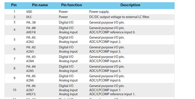
1.在nrf51822 中有8个模拟通道,如下图所示。当然P0.26和P0.27也可以做ADC引脚,这2个脚是时钟信号输入脚
2.在实验中我们用到P04作为模拟脚。用查询的模式来采集adc值(并非中断)
a.首先配置管脚,把管教配置为输入
#define ADC_PIN 									(4U)
#define ADC_INPUT()	nrf_gpio_cfg_input(ADC_PIN, NRF_GPIO_PIN_NOPULL)
b.采集adc值
/* Peripheral: ADC */
/* Description: Analog to digital converter. */

/* Register: ADC_INTENSET */
/* Description: Interrupt enable set register. */

/* Bit 0 : Enable interrupt on END event. */
#define ADC_INTENSET_END_Pos (0UL) /*!< Position of END field. */
#define ADC_INTENSET_END_Msk (0x1UL << ADC_INTENSET_END_Pos) /*!< Bit mask of END field. */
#define ADC_INTENSET_END_Disabled (0UL) /*!< Interrupt disabled. */
#define ADC_INTENSET_END_Enabled (1UL) /*!< Interrupt enabled. */
#define ADC_INTENSET_END_Set (1UL) /*!< Enable interrupt on write. */

/* Register: ADC_INTENCLR */
/* Description: Interrupt enable clear register. */

/* Bit 0 : Disable interrupt on END event. */
#define ADC_INTENCLR_END_Pos (0UL) /*!< Position of END field. */
#define ADC_INTENCLR_END_Msk (0x1UL << ADC_INTENCLR_END_Pos) /*!< Bit mask of END field. */
#define ADC_INTENCLR_END_Disabled (0UL) /*!< Interrupt disabled. */
#define ADC_INTENCLR_END_Enabled (1UL) /*!< Interrupt enabled. */
#define ADC_INTENCLR_END_Clear (1UL) /*!< Disable interrupt on write. */

/* Register: ADC_BUSY */
/* Description: ADC busy register. */

/* Bit 0 : ADC busy register. */
#define ADC_BUSY_BUSY_Pos (0UL) /*!< Position of BUSY field. */
#define ADC_BUSY_BUSY_Msk (0x1UL << ADC_BUSY_BUSY_Pos) /*!< Bit mask of BUSY field. */
#define ADC_BUSY_BUSY_Ready (0UL) /*!< No ongoing ADC conversion is taking place. ADC is ready. */
#define ADC_BUSY_BUSY_Busy (1UL) /*!< An ADC conversion is taking place. ADC is busy. */

/* Register: ADC_ENABLE */
/* Description: ADC enable. */

/* Bits 1..0 : ADC enable. */
#define ADC_ENABLE_ENABLE_Pos (0UL) /*!< Position of ENABLE field. */
#define ADC_ENABLE_ENABLE_Msk (0x3UL << ADC_ENABLE_ENABLE_Pos) /*!< Bit mask of ENABLE field. */
#define ADC_ENABLE_ENABLE_Disabled (0x00UL) /*!< ADC is disabled. */
#define ADC_ENABLE_ENABLE_Enabled (0x01UL) /*!< ADC is enabled. If an analog input pin is selected as source of the conversion, the selected pin is configured as an analog input. */

/* Register: ADC_CONFIG */
/* Description: ADC configuration register. */

/* Bits 17..16 : ADC external reference pin selection. */
#define ADC_CONFIG_EXTREFSEL_Pos (16UL) /*!< Position of EXTREFSEL field. */
#define ADC_CONFIG_EXTREFSEL_Msk (0x3UL << ADC_CONFIG_EXTREFSEL_Pos) /*!< Bit mask of EXTREFSEL field. */
#define ADC_CONFIG_EXTREFSEL_None (0UL) /*!< Analog external reference inputs disabled. */
#define ADC_CONFIG_EXTREFSEL_AnalogReference0 (1UL) /*!< Use analog reference 0 as reference. */
#define ADC_CONFIG_EXTREFSEL_AnalogReference1 (2UL) /*!< Use analog reference 1 as reference. */

/* Bits 15..8 : ADC analog pin selection. */
#define ADC_CONFIG_PSEL_Pos (8UL) /*!< Position of PSEL field. */
#define ADC_CONFIG_PSEL_Msk (0xFFUL << ADC_CONFIG_PSEL_Pos) /*!< Bit mask of PSEL field. */
#define ADC_CONFIG_PSEL_Disabled (0UL) /*!< Analog input pins disabled. */
#define ADC_CONFIG_PSEL_AnalogInput0 (1UL) /*!< Use analog input 0 as analog input. */
#define ADC_CONFIG_PSEL_AnalogInput1 (2UL) /*!< Use analog input 1 as analog input. */
#define ADC_CONFIG_PSEL_AnalogInput2 (4UL) /*!< Use analog input 2 as analog input. */
#define ADC_CONFIG_PSEL_AnalogInput3 (8UL) /*!< Use analog input 3 as analog input. */
#define ADC_CONFIG_PSEL_AnalogInput4 (16UL) /*!< Use analog input 4 as analog input. */
#define ADC_CONFIG_PSEL_AnalogInput5 (32UL) /*!< Use analog input 5 as analog input. */
#define ADC_CONFIG_PSEL_AnalogInput6 (64UL) /*!< Use analog input 6 as analog input. */
#define ADC_CONFIG_PSEL_AnalogInput7 (128UL) /*!< Use analog input 7 as analog input. */

/* Bits 6..5 : ADC reference selection. */
#define ADC_CONFIG_REFSEL_Pos (5UL) /*!< Position of REFSEL field. */
#define ADC_CONFIG_REFSEL_Msk (0x3UL << ADC_CONFIG_REFSEL_Pos) /*!< Bit mask of REFSEL field. */
#define ADC_CONFIG_REFSEL_VBG (0x00UL) /*!< Use internal 1.2V bandgap voltage as reference for conversion. */
#define ADC_CONFIG_REFSEL_External (0x01UL) /*!< Use external source configured by EXTREFSEL as reference for conversion. */
#define ADC_CONFIG_REFSEL_SupplyOneHalfPrescaling (0x02UL) /*!< Use supply voltage with 1/2 prescaling as reference for conversion. Only usable when supply voltage is between 1.7V and 2.6V. */
#define ADC_CONFIG_REFSEL_SupplyOneThirdPrescaling (0x03UL) /*!< Use supply voltage with 1/3 prescaling as reference for conversion. Only usable when supply voltage is between 2.5V and 3.6V. */

/* Bits 4..2 : ADC input selection. */
#define ADC_CONFIG_INPSEL_Pos (2UL) /*!< Position of INPSEL field. */
#define ADC_CONFIG_INPSEL_Msk (0x7UL << ADC_CONFIG_INPSEL_Pos) /*!< Bit mask of INPSEL field. */
#define ADC_CONFIG_INPSEL_AnalogInputNoPrescaling (0x00UL) /*!< Analog input specified by PSEL with no prescaling used as input for the conversion. */
#define ADC_CONFIG_INPSEL_AnalogInputTwoThirdsPrescaling (0x01UL) /*!< Analog input specified by PSEL with 2/3 prescaling used as input for the conversion. */
#define ADC_CONFIG_INPSEL_AnalogInputOneThirdPrescaling (0x02UL) /*!< Analog input specified by PSEL with 1/3 prescaling used as input for the conversion. */
#define ADC_CONFIG_INPSEL_SupplyTwoThirdsPrescaling (0x05UL) /*!< Supply voltage with 2/3 prescaling used as input for the conversion. */
#define ADC_CONFIG_INPSEL_SupplyOneThirdPrescaling (0x06UL) /*!< Supply voltage with 1/3 prescaling used as input for the conversion. */

/* Bits 1..0 : ADC resolution. */
#define ADC_CONFIG_RES_Pos (0UL) /*!< Position of RES field. */
#define ADC_CONFIG_RES_Msk (0x3UL << ADC_CONFIG_RES_Pos) /*!< Bit mask of RES field. */
#define ADC_CONFIG_RES_8bit (0x00UL) /*!< 8bit ADC resolution. */
#define ADC_CONFIG_RES_9bit (0x01UL) /*!< 9bit ADC resolution. */
#define ADC_CONFIG_RES_10bit (0x02UL) /*!< 10bit ADC resolution. */
/**@brief Function for making the ADC start a battery level conversion.
 */
 uint16_t adc_start(void)
{
    uint32_t err_code;
    uint8_t times = 0 ;
    uint16_t adc_result = 0;
	  ADC_INPUT();
    // Configure ADC
    NRF_ADC->INTENSET   = ADC_INTENSET_END_Msk;
    NRF_ADC->CONFIG     = (ADC_CONFIG_RES_10bit                        << ADC_CONFIG_RES_Pos)     |
                          (ADC_CONFIG_INPSEL_AnalogInputOneThirdPrescaling << ADC_CONFIG_INPSEL_Pos)  |
                          (ADC_CONFIG_REFSEL_VBG    << ADC_CONFIG_REFSEL_Pos)  |
                          (ADC_CONFIG_PSEL_AnalogInput5                  << ADC_CONFIG_PSEL_Pos)    |
                          (ADC_CONFIG_EXTREFSEL_None                  << ADC_CONFIG_EXTREFSEL_Pos);
    NRF_ADC->EVENTS_END = 0;
    NRF_ADC->ENABLE     = ADC_ENABLE_ENABLE_Enabled;

    // Enable ADC interrupt
    err_code = sd_nvic_ClearPendingIRQ(ADC_IRQn);
    APP_ERROR_CHECK(err_code);

    err_code = sd_nvic_SetPriority(ADC_IRQn, NRF_APP_PRIORITY_LOW);
    APP_ERROR_CHECK(err_code);

  	err_code =sd_nvic_DisableIRQ(ADC_IRQn);
   // err_code = sd_nvic_EnableIRQ(ADC_IRQn);
    APP_ERROR_CHECK(err_code);

    NRF_ADC->EVENTS_END  = 0;    // Stop any running conversions.
    NRF_ADC->TASKS_START = 1;
		 while (NRF_ADC->EVENTS_END == 0 || times >200 )
    {
			times ++ ;
		}
		if(times > 200)
		{
		//	ת»»Ê§°Ü
		}else
		{
		NRF_ADC->EVENTS_END     = 0;
		adc_result              = NRF_ADC->RESULT;
		NRF_ADC->TASKS_STOP     = 1;
		}
    return 			adc_result;
}
NRF_ADC->CONFIG = (ADC_CONFIG_RES_10bit << ADC_CONFIG_RES_Pos) |
(ADC_CONFIG_INPSEL_AnalogInputOneThirdPrescaling << ADC_CONFIG_INPSEL_Pos) |
(ADC_CONFIG_REFSEL_VBG << ADC_CONFIG_REFSEL_Pos) |
(ADC_CONFIG_PSEL_AnalogInput5 << ADC_CONFIG_PSEL_Pos) |
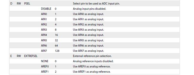
(ADC_CONFIG_EXTREFSEL_None << ADC_CONFIG_EXTREFSEL_Pos);选择的是 1.10位的adc (通过程序可以选择8 ,9 ,10位) 2.模拟脚的1/3作为输入。 3.1.2v作为参考电压。 4.选择模拟通道5 5.不用外部参考源 具体配置如下寄存器选择。 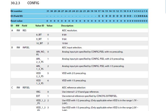
具体请参考nrf51822数据手册
用万用表量出的值为2.36v
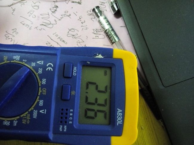
采集出来的adc为
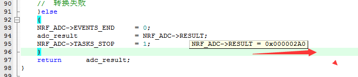
0x2a0/1024.0*1.2*3 =2.3625与量出的结果一样。说明采集正确
完毕!!!