IIC总线接口基础知识
原文链接:IIC总线接口基础知识
目录
1、I2C Interface
1.1 、 I2C Enable / Disable
1.2、 Start & Stop Condition
1.3 、Data validity
1.4、 Byte Format
1.5 、Acknowledge
2、 First Byte
2.1、 Slave Address
2.2、 R/W(头上有个横杠代表低电平有效)
3、 Transferring Data
3.1、 Write Operation
3.2、Read Operation
3.3、 Read/Write Operation
4、 I2C write and read operations in normal mode
1、I2C Interface
1.1 、 I2C Enable / Disable
If the SDA or SCL signal goes to low, I2C control block is enabled automatically. And if the SDA and SCL signal maintain high during about 2 us, I2C control block is disabled automatically also.
如果SDA或SCL信号变为低电平,则自动启用I2C控制模块。 如果SDA和SCL信号在大约2 us期间保持高电平,I2C控制模块也自动禁用。
1.2、 Start & Stop Condition
- Start Condition (S)
- Stop Condition (P)
- Repeated Start (Sr)
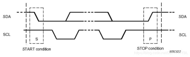
当SCL保持再高电平,SDA由高电平变为低电平为开始信号。
当SCL保持在高电平,SDA由低电平变为高电平为停止信号。
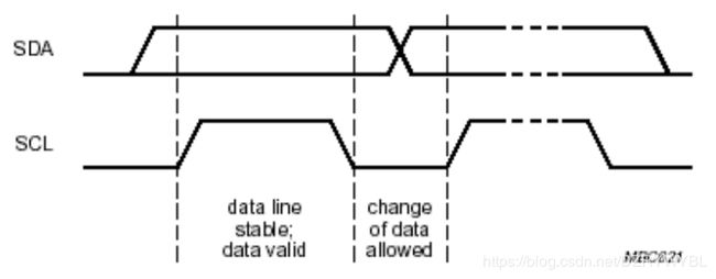
1.3 、Data validity
The SDA should be stable when the SCL is high and the SDA can be changed when the SCL is low.
当SCL为高电平时,SDA应保持稳定,当SCL为低电平时,SDA可以更改。
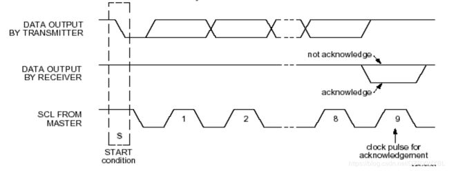
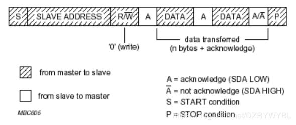
1.4、 Byte Format
The byte structure is composed with 8Bit data and an acknowledge signal.
字节结构由8Bit数据和确认信号组成。
1.5 、Acknowledge
It is a check bit whether the receiver gets the data from the transmitter without error or not. The receiver will write ‘0’ when it received the data successfully and ‘1’ if not.
检测接收器是否有无错误地从发送器获取数据。 接收器在成功接收数据时写入“0”,否则写入“1”。
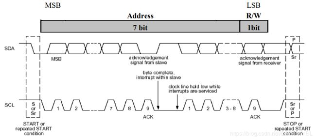
2、 First Byte
2.1、 Slave Address
It is the first byte from the start condition. It is used to access the slave device.
它是起始条件后的第一个字节。 它用于访问从设备。列举一个ADSTS20触摸芯片的例子。
TS20 Chip Address : 7bit
| ADD | Address |
| GND | 0xD4 |
| VSS | 0xF4 |
ADD是从地址选择脚,ADD接地(GND),从地址就是0xD4,ADD接电源(VSS),从地址就是0xF4。
2.2、 R/W(头上有个横杠代表低电平有效)
The direction of data is decided by the bit and it follows the address data.
这个位决定数据的方向(发送或者接收),它紧跟着从地址。
R/W = 1 ;代表要从从地址读数据,反之则是要写数据。
3、 Transferring Data
3.1、 Write Operation
The byte sequence is as follows:
- The first byte gives the device address plus the direction bit (R/W = 0).
- The second byte contains the internal address of the first register to be accessed.
- The next byte is written in the internal register. Following bytes are written in successive internal registers.
- The transfer lasts until stop conditions are encountered.
- The TS20 acknowledges every byte transfer.
字节序列如下:(这里看不懂没关系,后面Write操作的例程)
- 第一个字节给出器件地址加方向位(R / W = 0)。
- 第二个字节,简单说就是主机要访问从设备的寄存器的首地址。比如是0x05,就是从第五个寄存器开始访问。
- 后面传送的数据都会写入从设备内部寄存器中,从第二个步骤传送的地址开始写入。
- 转移持续到遇到停止条件。
- TS20确认每个字节传输。
3.2、Read Operation
The address of the first register to read is programmed in a write operation without data, and terminated by the
stop condition. Then, another start is followed by the device address and R/W= 1. All following bytes are now
data to be read at successive positions starting from the initial address.
简而言之就是说,想要读取一个数据,就要先用写命令(R/W = 0)将从设备的地址和第一个要读取的寄存器地址给传送出去,后面不传送数据直接发送停止信号。然后就可以用读命令从上一步骤发送的寄存器地址开始读取数据了。

3.3、 Read/Write Operation

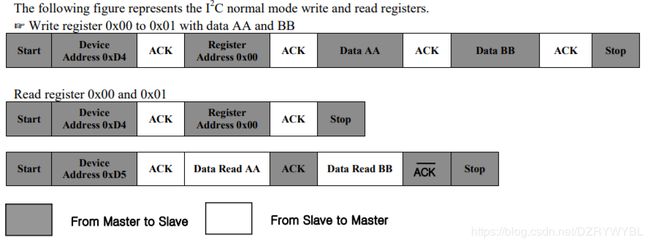
4、 I2C write and read operations in normal mode
我觉得下面这个例程看懂了,再去理解上面的就很容易了。
欢迎交流......